IGBT device with a groove gate type JFET structure

A grooved gate and gate structure technology, which is applied in the fields of semiconductor devices, semiconductor/solid-state device manufacturing, electrical components, etc., can solve the problems of reducing the turn-off capability of the device, increasing the turn-off loss of the device, and damaging the breakdown voltage of the device. , to reduce the saturated turn-on voltage drop and turn-off loss, reduce the gate resistance, and improve the turn-off capability.

Active Publication Date: 2018-11-06
UNIV OF ELECTRONICS SCI & TECH OF CHINA
View PDF3 Cites 4 Cited by
  • Summary
  • Abstract
  • Description
  • Claims
  • Application Information

AI Technical Summary

Problems solved by technology

However, the FP region between the trench gates stores excess holes during forward conduction, which will introduce negative gate capacitance effect to generate displacement current in the gate, which affects the gate control ability; it takes time for the hole current to discharge when it is turned off, making the device The turn-off loss increases
At the same time, if the holes cannot be extracted from the FP region in time during the turn-off process, the leakage current after turn-off will be too large, which will induce delayed failure and reduce the turn-off capability of the device.
The existing solution provides a discharge path for holes in the FP region when it is turned off by introducing clamping diodes and diffusion resistors, but it exposes problems such as low discharge efficiency and damaged device breakdown voltage.

Method used


Image

  • IGBT device with a groove gate type JFET structure
  • IGBT device with a groove gate type JFET structure

Examples


Embodiment

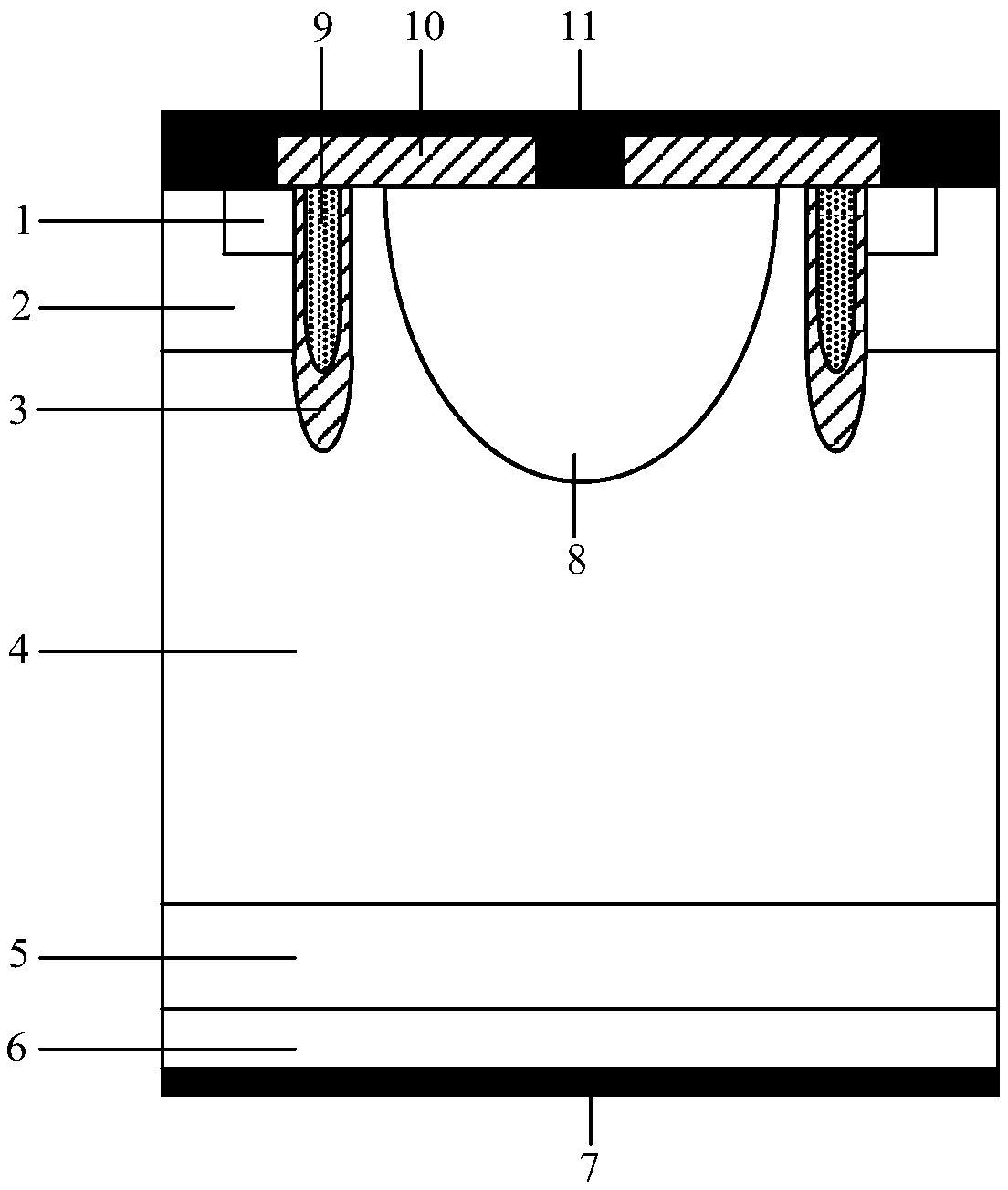
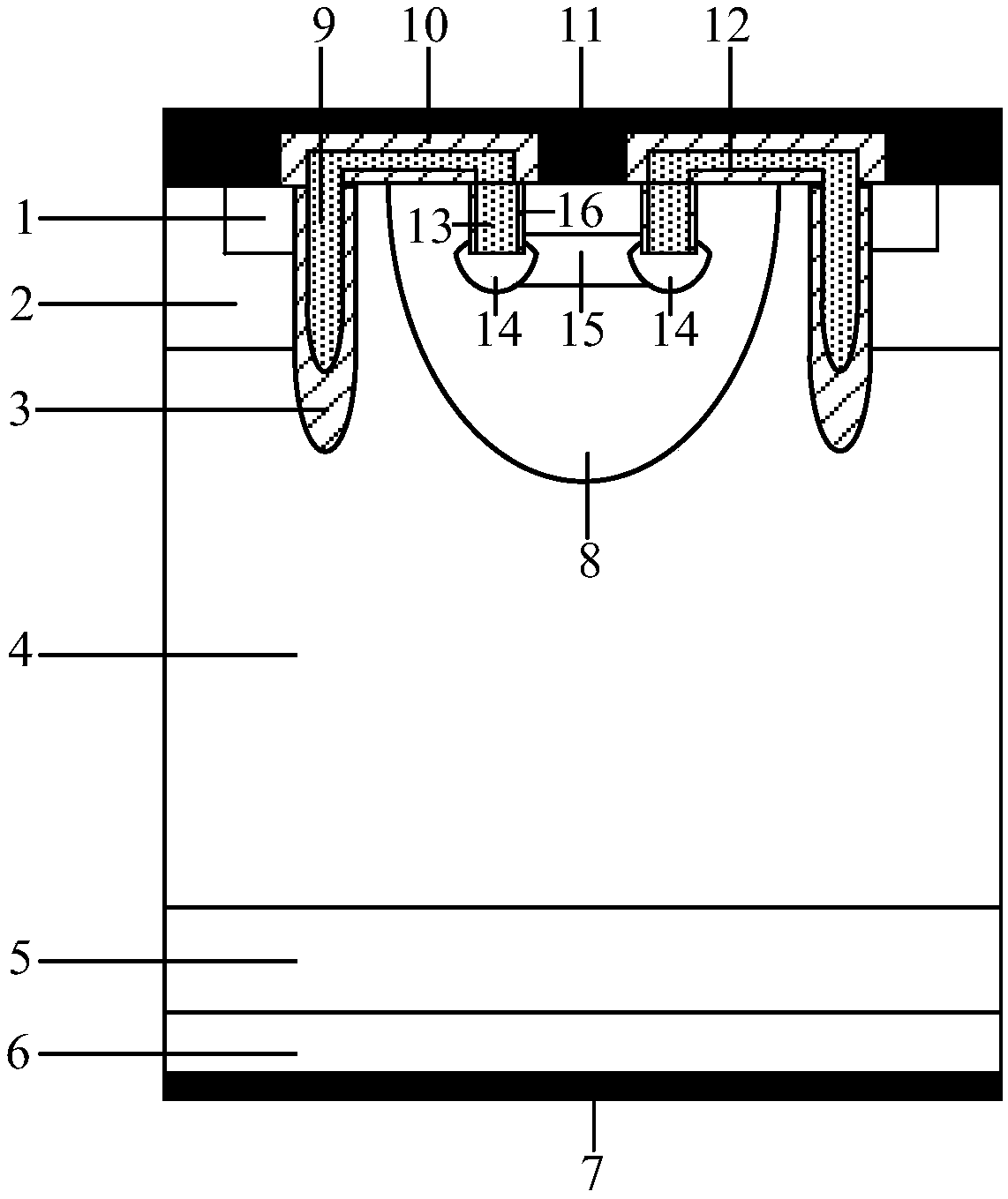
[0029] An IGBT device with a groove gate JFET structure, such as figure 2As shown, its cellular structure includes a metal collector 7, a first conductivity type semiconductor collector region 6, a second conductivity type semiconductor buffer layer 5, a second conductivity type semiconductor drift region 4, and a metal emitter stacked sequentially from bottom to top. pole 11; the top layer of the second conductivity type semiconductor drift region 4 has a first conductivity type semiconductor body region 8, a first conductivity type semiconductor base region 2, a second conductivity type semiconductor emitter region 1 and a first gate structure; The first conductivity type semiconductor body region 8 is located in the middle region of the top layer of the second conductivity type semiconductor drift region 4; the first conductivity type semiconductor base region 2 is respectively located in the regions on both sides of the second conductivity type semiconductor drift region 4...


PUM


Abstract

The invention relates to an IGBT device with a groove gate type JFET structure, belonging to the technical field of power semiconductor devices. A JFET region equivalent to a JFET variable resistanceis introduced into a neutral region other than a depletion region generated in a forward block body region of the device, The holes are stored when the device is turned on forward, and a quick discharging loop is provided for the holes when the device is blocked forward, so that the saturation conduction voltage drop and the shutdown loss of the device are reduced, the short-circuit failure phenomenon after the device is turned off is avoided, and the shutdown ability of the device is improved. Moreover, the connection bridge between the gate structure and the JFET region can act as a field plate when the device is blocked in the forward direction, so that the surface electric field peak value under the connection bridge can be effectively reduced, and the withstand voltage and the workingreliability of the device can be improved. The manufacturing method of the IGBT device with a groove gate type JFET structure is compatible with that of the prior art. A JFET region is fabricated bya shallow groove etching and ion implantation process, which is conducive to reducing the gate resistance of the JFET region and enhancing the gate control ability of the JFET structure; it is helpfulto reduce the size of the JFET structure, increase cell density and realize industrial production.

Description

technical field [0001] The invention belongs to the technical field of power semiconductor devices, and in particular relates to an IGBT device with a groove gate JFET structure. Background technique [0002] With the rapid development of rail transit, smart grid, green energy and other fields, insulated gate bipolar transistor (Insulated Gate Bipolar Transistor, IGBT) has simple gate control, high input impedance, fast switching speed, high current density, saturation voltage It has become one of the mainstream power switching devices in the field of medium and high power power electronics; at the same time, it will continue to develop in the direction of high voltage, high current, high operating temperature and high reliability. The application of IGBT devices in high-voltage applications, especially in the process of motor driving, will experience a short circuit at both ends of the device; the device will be turned on when the load is short-circuited, resulting in a sho...

Claims


Application Information

Patent Timeline
Patent Type & Authority Applications(China)
IPC IPC(8): H01L29/06H01L29/40H01L29/739H01L21/331
CPCH01L29/0684H01L29/405H01L29/66348H01L29/7397H01L29/7398
Inventor 李泽宏彭鑫殷鹏飞杨洋张金平高巍任敏张波
Owner UNIV OF ELECTRONICS SCI & TECH OF CHINA
Why Eureka
Try Eureka