A kind of thin film transistor and its manufacturing method, array substrate, display device

A technology for thin film transistors and array substrates, applied in the fields of display devices, thin film transistors and their fabrication methods, and array substrates, can solve the problems of inability to accurately optical compensation, inability to guarantee signal-to-noise ratio, negative threshold voltage drift, etc., and to reduce leakage current , Avoid negative drift of threshold voltage and ensure the effect of reducing dark current

Active Publication Date: 2021-09-21
BOE TECH GRP CO LTD
View PDF6 Cites 0 Cited by
  • Summary
  • Abstract
  • Description
  • Claims
  • Application Information

AI Technical Summary

Problems solved by technology

However, the PIN diode will produce more hydrogen atoms during the manufacturing process, and these hydrogen atoms will erode the channel region of the active layer of the thin film transistor, causing the threshold voltage of the TFT to drift negatively, and the leakage current increases, resulting in a dark current during optical detection. Large, the signal-to-noise ratio cannot be guaranteed, and optical compensation cannot be performed accurately

Method used


Image

  • A kind of thin film transistor and its manufacturing method, array substrate, display device
  • A kind of thin film transistor and its manufacturing method, array substrate, display device
  • A kind of thin film transistor and its manufacturing method, array substrate, display device

Examples


Embodiment 1

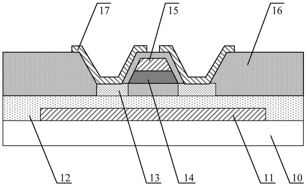
[0068] figure 1 Schematic structure of the thin film transistor provided for the embodiment of the present invention Figure 1 ;Such as figure 1 As shown, the thin film transistor provided by the embodiment of the present invention includes: a first gate 11 disposed on one side of the substrate 10 , an active layer 13 , a second gate 15 and source-drain electrodes 17 .

[0069] Wherein, the active layer 13 is arranged on the side of the first gate 11 away from the base substrate 10; the second gate 15 is arranged on the side of the active layer 13 away from the base substrate 10; the source and drain electrodes 17 are arranged on the second The side of the gate 15 away from the base substrate 10 ; the orthographic projection of the source and drain electrodes 17 on the base substrate 10 overlaps with the orthographic projection of the second gate 15 on the base substrate 10 .

[0070] It should be noted that, if figure 1 As shown, the thin film transistor provided by the em...

Embodiment 2

[0095] Based on the inventive concepts of the above embodiments, the embodiments of the present invention also provide a method for manufacturing a thin film transistor, Figure 5 The flow chart of the manufacturing method of the thin film transistor provided by the embodiment of the present invention, such as Figure 5 As shown, the manufacturing method of the thin film transistor provided in the embodiment of the present invention specifically includes the following steps:

[0096] Step 100, providing a base substrate.

[0097] Optionally, the base substrate may be a transparent insulating substrate, such as a glass substrate, a quartz substrate or other suitable substrates, which is not limited in this embodiment of the present invention.

[0098] Step 200, forming a first gate on one side of the substrate.

[0099] Optionally, the manufacturing material of the first gate may include copper-based metal, aluminum-based metal, and nickel-based technology. For example, the ...

Embodiment 3

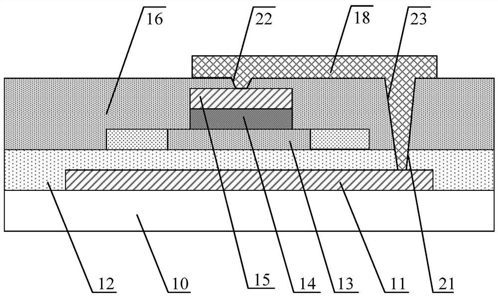
[0153] Based on the inventive concepts of the above embodiments, the embodiments of the present invention further provide an array substrate, Figure 7 Schematic diagram of the structure of the array substrate provided for the embodiment of the present invention Figure 1 ,Such as Figure 7 As shown, the array substrate provided by the embodiment of the present invention includes a thin film transistor 1 and a photosensitive element 2 .

[0154] Wherein, the thin film transistor 1 is the thin film transistor provided in the first embodiment.

[0155] Specifically, the photosensitive element 2 is arranged on the side where the source and drain electrodes of the thin film transistor 1 are away from the substrate; the first electrode 2a of the photosensitive element 2 is connected to the source electrode or the drain electrode of the thin film transistor 1 .

[0156] Optionally, the photosensitive element 2 can be a PIN diode.

[0157] Optionally, as in Figure 7 As shown, th...


PUM


Abstract

The embodiment of the present invention discloses a thin film transistor and its manufacturing method, an array substrate, and a display device, wherein the thin film transistor includes: a first gate arranged on one side of the substrate, an active layer, a second gate, and a source-drain circuit wherein, the active layer is arranged on the side of the first gate away from the substrate; the second gate is arranged on the side of the first gate away from the substrate; the source and drain electrodes are arranged on the side of the second gate away from the substrate One side of the base substrate; there is an overlapping area between the orthographic projection of the source and drain electrodes on the base substrate and the orthographic projection of the second gate on the base substrate. The embodiment of the present invention prevents hydrogen atoms from entering the active layer in the subsequent process, avoids the negative drift of the threshold voltage of the thin film transistor, reduces the leakage current of the thin film transistor, and then ensures that the dark current becomes smaller and the signal-to-noise ratio during optical detection can be accurately detected. Optically compensates the display.

Description

technical field [0001] Embodiments of the present invention relate to the field of display technology, and in particular to a thin film transistor and a manufacturing method thereof, an array substrate, and a display device. Background technique [0002] Organic Light-Emitting Diode (OLED) is one of the hot spots in the field of flat panel display research. Compared with Liquid Crystal Display (LCD), OLED display has low energy consumption, low production cost, self-luminous , wide viewing angle and fast response speed, etc. At present, OLED displays have begun to replace traditional LCD displays in the display fields of mobile phones, tablet computers, and digital cameras. [0003] The problem of brightness attenuation will occur in the working process of OLED display. In order to ensure the uniform and continuous brightness of the display, it is necessary to adopt a suitable compensation method, one of which is optical compensation. Optical compensation is a method that u...

Claims


Application Information

Patent Timeline
Patent Type & Authority Patents(China)
IPC IPC(8): H01L29/786H01L29/417H01L21/34H01L21/44H01L27/12H01L27/32
CPCH01L27/1214H01L29/41733H01L29/41775H01L29/66969H01L29/78648H01L29/7869H01L21/44H10K59/60H10K59/12H01L29/78633H01L29/78696H10K59/123H10K59/13H10K59/126H01L23/5226H01L27/1225
Inventor 王玲林奕呈盖翠丽徐攀
Owner BOE TECH GRP CO LTD
Why Eureka
Try Eureka