Spectrum selective emission material that can be used for infrared stealth and its preparation method
An emission material and selective technology, applied in chemical instruments and methods, metal material coating technology, optics, etc., can solve the problems of inconvenient large-area preparation, material layer falling off, low-emissivity infrared stealth film, etc., to achieve convenient Large-area preparation and application, low emissivity and radiation heat dissipation, simple and feasible preparation process
- Summary
- Abstract
- Description
- Claims
- Application Information
AI Technical Summary
Problems solved by technology
Method used
Image
Examples
Embodiment 1
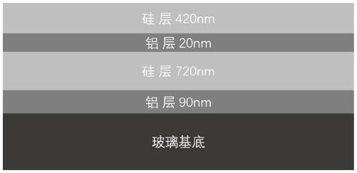
[0030] a kind of like figure 1 The spectrally selective emission material that can be used for infrared stealth is shown. The spectrally selective emission material is a layered structure that can regulate the emission characteristics of the infrared spectrum. The layered structure uses glass as a substrate, and the glass surface is alternately coated There are metal layers and infrared transparent dielectric layers.
[0031] In the spectrally selective emission material of this embodiment, the metal layer is an Al layer, and the infrared transparent medium layer is Si. The material in this embodiment is composed of metal layers and infrared transparent medium layers alternately stacked and compounded, and there are four layers in total. Starting from the substrate layer, there are 90nm Al layer, 720nm Si layer, 20nm Al layer, and 420nm Si layer in sequence, and the total thickness of the entire layered structure is 1250.0nm.
[0032] In this embodiment, the infrared transmi...
Embodiment 2
[0037] A spectrally selective emission material that can be used for infrared stealth. The spectrally selective emission material is a layered structure that can regulate the emission radiation characteristics of the infrared spectrum. The layered structure uses a silicon wafer as a substrate, and the surface of the silicon wafer is coated with Covered with a metal layer and an infrared transparent medium layer.
[0038] In the spectrally selective emission material of this embodiment, the metal layer is W, and the infrared transparent medium layer is ZnSe. The layered structure of this embodiment is composed of W metal layers and ZnSe dielectric layers alternately stacked and compounded. From the silicon wafer substrate, they are 50.0nm W, 800.0nm ZnSe, 18nm W, and 500.0nm ZnSe. The total thickness of the entire layered structure is 1368.0nm.
[0039] In this embodiment, the infrared transmittance of the 500nm and 800nm infrared transparent medium layer ZnSe is higher than...
PUM
| Property | Measurement | Unit |
|---|---|---|
| thickness | aaaaa | aaaaa |
| thickness | aaaaa | aaaaa |
| thickness | aaaaa | aaaaa |
Abstract
Description
Claims
Application Information


