Two-dimensional semiconductor material negative capacitance field effect transistor and preparation method thereof

A two-dimensional semiconductor and capacitive field technology, applied in the field of nanoelectronics, can solve the problems of serious interface state and deteriorating subthreshold slope of the device, and achieve the effects of small contact resistance, improved Fermi pinning of metal contacts, and simple preparation process

Active Publication Date: 2018-11-16
PEKING UNIV
View PDF7 Cites 7 Cited by
  • Summary
  • Abstract
  • Description
  • Claims
  • Application Information

AI Technical Summary

Problems solved by technology

However, most of the gate dielectric materials of field effect transistors based on two-dimensional materials are still realized by atomic layer deposition. The interface s

Method used


Image

  • Two-dimensional semiconductor material negative capacitance field effect transistor and preparation method thereof
  • Two-dimensional semiconductor material negative capacitance field effect transistor and preparation method thereof
  • Two-dimensional semiconductor material negative capacitance field effect transistor and preparation method thereof

Examples


Example Embodiment

[0043] In the following, the present invention will be further described through embodiments with reference to the accompanying drawings.

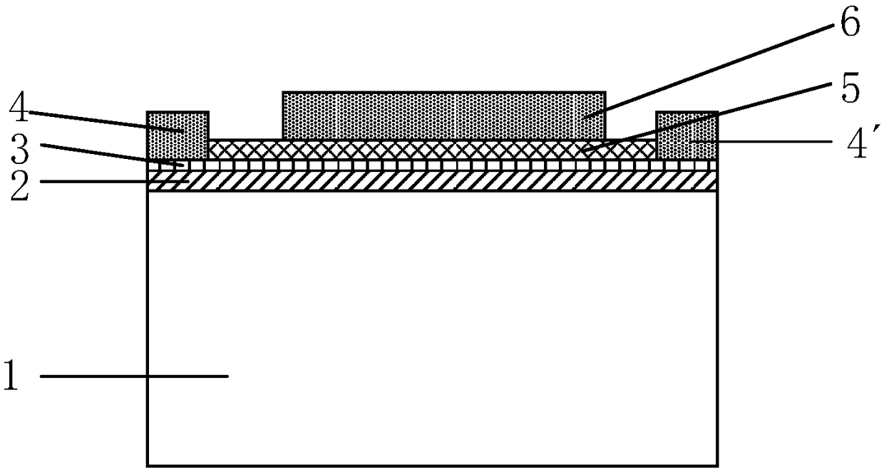
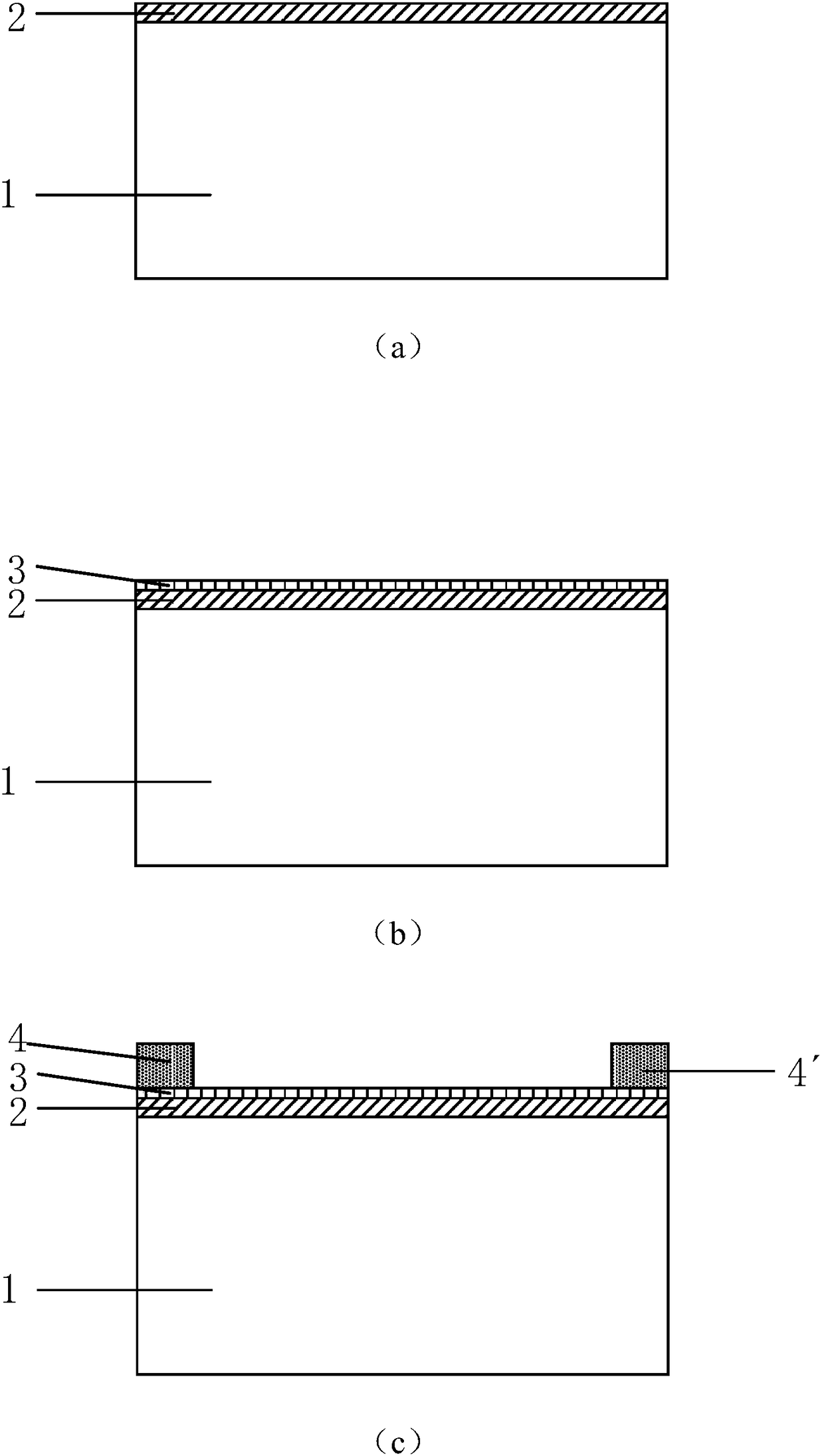
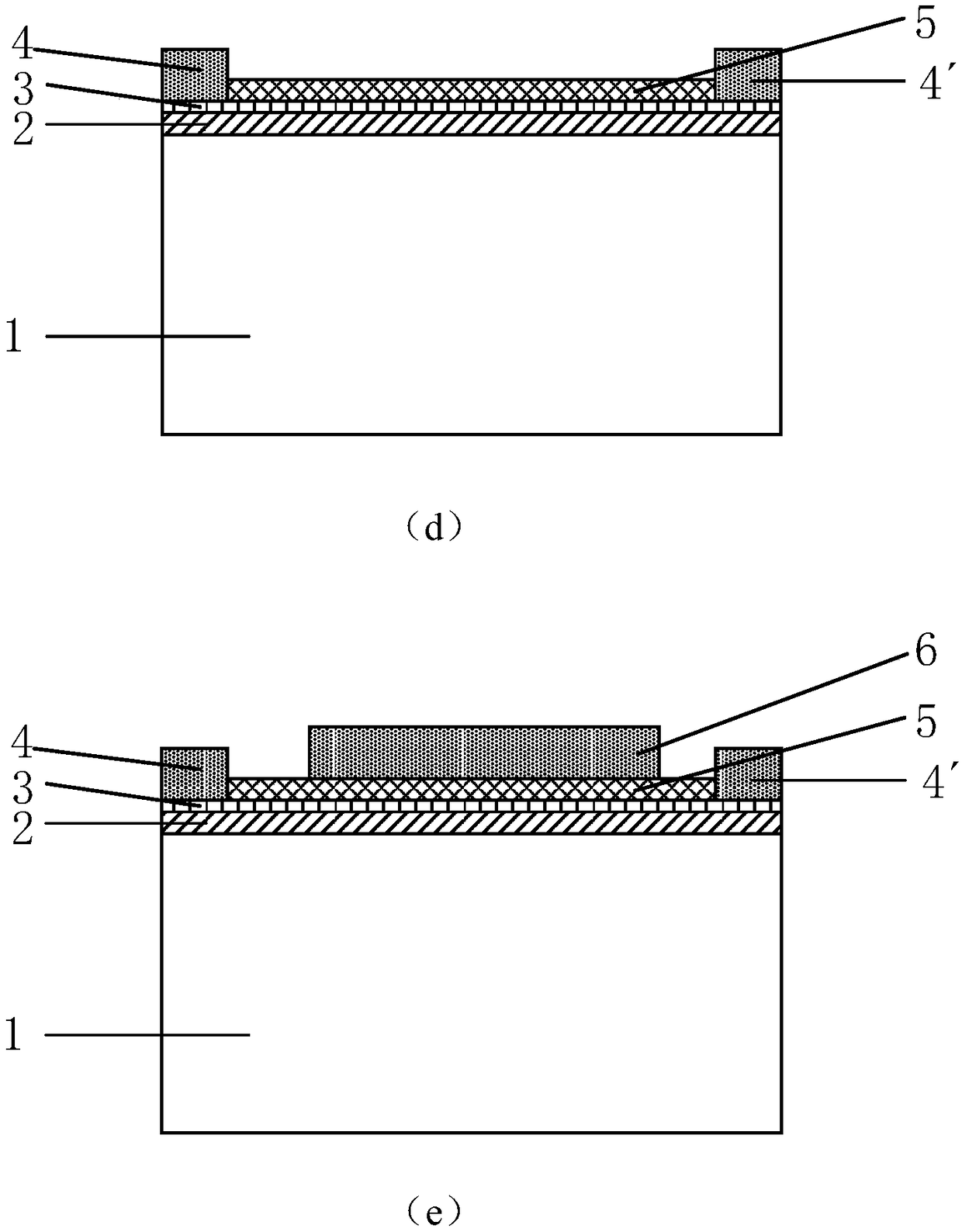
[0044] Such as figure 1 As shown, the negative capacitance field effect transistor based on the two-dimensional semiconductor material of the present invention includes an insulating substrate 1 and a two-dimensional alloy semiconductor material HfZrSe 2 Layer 2, a HfZrO with ferroelectric properties 2 The dielectric layer 3, a metal source electrode 4, a metal drain electrode 4', a high-k gate dielectric layer 5, and a control gate electrode 6. Among them, HfZrO with ferroelectric properties 2 The dielectric layer 3 is located in the two-dimensional alloy semiconductor material HfZrSe 2 Above layer 2, the metal source and drain electrodes 4 and 4'are located in HfZrO with ferroelectric properties 2 Above the dielectric layer 3, the high-k gate dielectric layer 5 is located between the metal source and drain electrodes. Two-dimensional alloy s...


PUM

PropertyMeasurementUnit
Thicknessaaaaaaaaaa
Thicknessaaaaaaaaaa
Thicknessaaaaaaaaaa

Abstract

The invention discloses a two-dimensional semiconductor material negative capacitance field effect transistor and a preparation method thereof; a two-dimensional alloy semiconductor material HfZrSe2 is adopted as a channel material, and the surface of the channel material is oxidized in air to generate HfZrO2, and then annealing is carried out to obtain an HfZrO2 dielectric layer with a ferroelectric property; a high-k gate dielectric layer is deposited on the dielectric layer, and a gate dielectric with a mixed structure is formed. By means of the device structure, high gate dielectric and channel two-dimensional semiconductor material interfaces can be obtained, the deterioration of the interface state on the sub-threshold characteristic is reduced, and the super-steep sub-threshold slope is easily obtained; meanwhile, the high-k gate dielectric on the upper layer can protect the HfZrO2 dielectric of the ferroelectric characteristics below, so that the dielectric is isolated from theair, and the stability of the device is greatly improved. The device is simple in preparation process and large-scale production can be realized.

Description

technical field [0001] The invention belongs to the technical field of nanoelectronics, and in particular relates to a two-dimensional semiconductor material negative capacitance field effect transistor and a preparation method thereof. Background technique [0002] With the reduction of traditional MOSFET feature size and the improvement of integration, the operating voltage and threshold voltage of the device are gradually reduced. The ensuing short-channel effect is more obvious, and the drain-induced barrier reduction and source-drain band-band tunneling will increase the leakage current and power consumption of the device. In addition, due to the current mechanism of MOSFET thermal emission, its subthreshold slope is limited by the thermal potential, and there is a theoretical limit of 60mV / dec, which cannot be reduced with the reduction of device size, which leads to a further increase in the leakage current of the device and power consumption. The problem intensifies...

Claims


Application Information

Patent Timeline
IPC IPC(8): H01L29/78H01L29/51H01L21/34H01L29/24
CPCH01L29/24H01L29/516H01L29/517H01L29/66969H01L29/78391
Inventor 黄如贾润东黄芊芊王慧敏陈亮杨勐譞
Owner PEKING UNIV
Why Eureka
Try Eureka