Method for preparing perovskite film, and perovskite solar cell device
A solar cell and perovskite technology, applied in the direction of electric solid devices, electrical components, semiconductor devices, etc., to achieve the effect of improving photovoltaic performance, improving charge transport capacity, increasing carrier mobility and diffusion length
- Summary
- Abstract
- Description
- Claims
- Application Information
AI Technical Summary
Problems solved by technology
Method used
Image

Examples
Embodiment 1
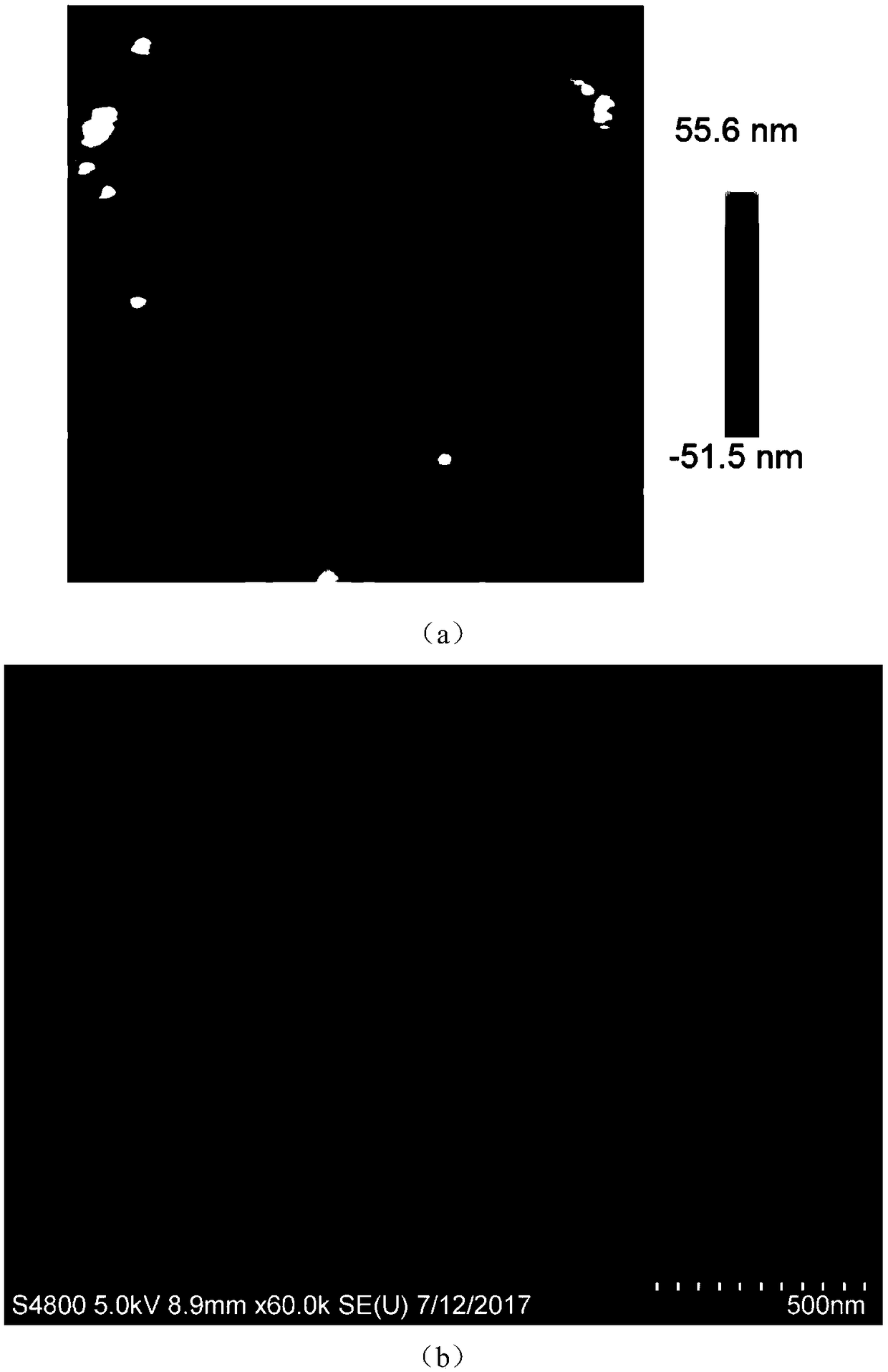
[0032] 1) Solution configuration: MAI and PbI 2Dissolve in the mixed solvent with a molar ratio of 1:1, the concentration is 1.5mmol / mL, DMF and DMSO in the mixed solvent form the main solution with the ratio of 8:2, and then add a certain volume of ether, so that the content of the ether additive accounts for 3% of the volume of the mixed solution, magnetic stirring for 6h until the solution is clear and ready for use;
[0033] 2) Cleaning of the substrate: place the ITO conductive glass substrate on a dedicated substrate holder, and use cleaning agent, deionized water, acetone and ethanol to ultrasonically twice, each time for 20 minutes; after cleaning, put it in an oven Dry, and then treat the dried ITO conductive glass with ultraviolet-ozone plasma for 4 minutes to improve the work function;
[0034] 3) Preparation of the hole transport layer: NiOx was made into a suspension with a concentration of 20 mg / mL, and it was dispersed more uniformly by ultrasonication before u...
Embodiment 2
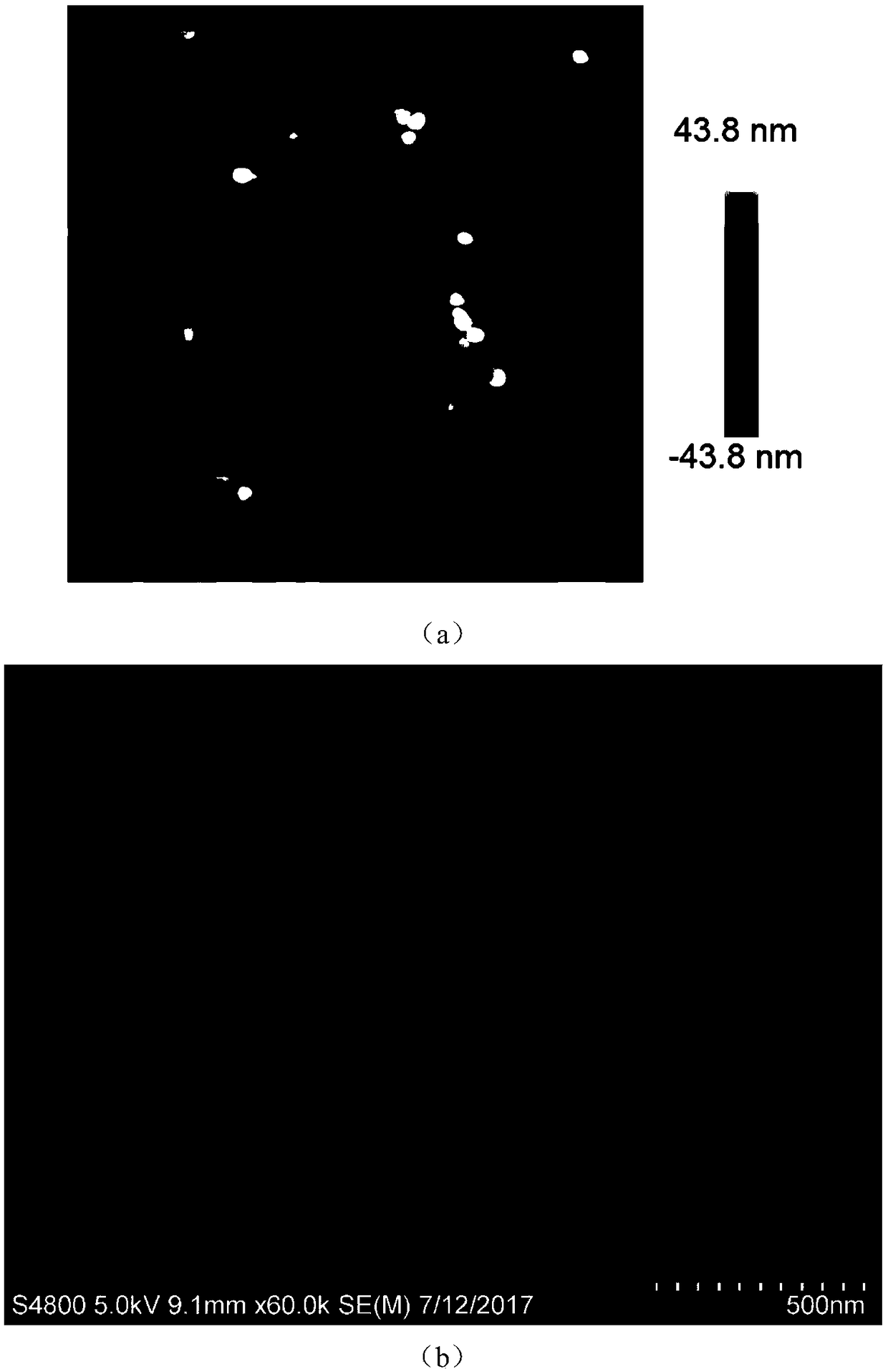
[0040] The perovskite thin film is prepared with reference to the method of Example 1, and the solar cell device is prepared with the perovskite thin film as the active layer, the difference is that in the perovskite precursor solution prepared in step 1), the volume of ether anti-solvent accounts for the total mixed solvent 4% of the volume.
Embodiment 3
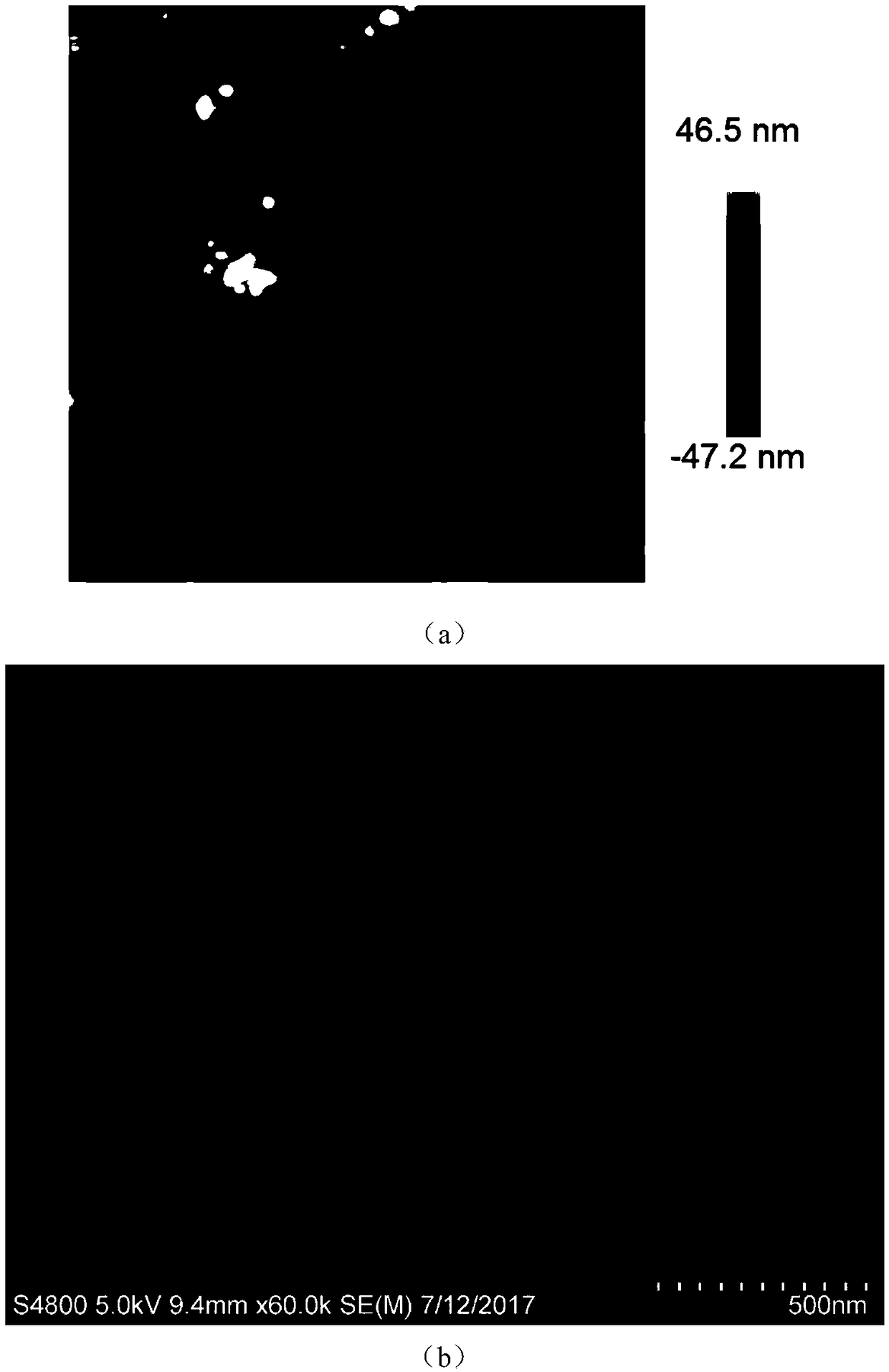
[0042] The perovskite thin film is prepared with reference to the method of Example 1, and the solar cell device is prepared with the perovskite thin film as the active layer, the difference is that in the perovskite precursor solution prepared in step 1), the volume of ether anti-solvent accounts for the total mixed solvent 6% of the volume.
PUM
| Property | Measurement | Unit |
|---|---|---|
| Thickness | aaaaa | aaaaa |
Abstract
Description
Claims
Application Information