Formation method of IGBT device, and structure of IGBT device

A device structure and device technology, applied in the field of IGBT device formation and its structure, can solve problems such as increased capacitance, achieve the effects of improving conduction voltage drop, increasing process window, and improving capacitance Cgc

Active Publication Date: 2018-12-07
SEMICON MFG INT (SHANGHAI) CORP +1
View PDF3 Cites 1 Cited by
  • Summary
  • Abstract
  • Description
  • Claims
  • Application Information

AI Technical Summary

Problems solved by technology

[0005] The object of the present invention is to provide a kind of forming method of IGBT device, when improving the anti-short circuit capabilit

Method used


Image

  • Formation method of IGBT device, and structure of IGBT device
  • Formation method of IGBT device, and structure of IGBT device
  • Formation method of IGBT device, and structure of IGBT device

Examples


Embodiment Construction

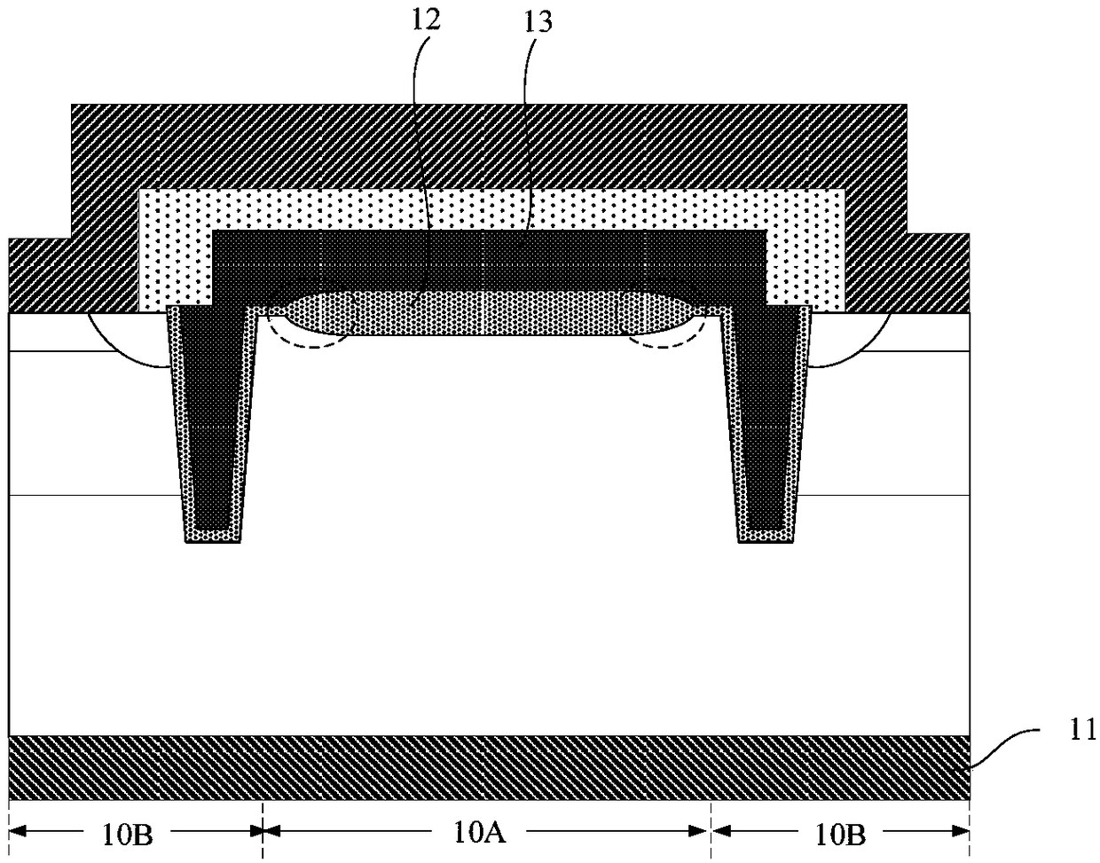
[0036] As mentioned in the background art, in trench type IGBT devices, a redundant cell (dummy cell) is formed between multiple functional cells to reduce the channel density, thereby improving the short-circuit resistance of the IGBT device. question. However, this method will correspondingly cause the capacitance Cgc between the gate and the collector to increase, thereby affecting the overall performance of the device.

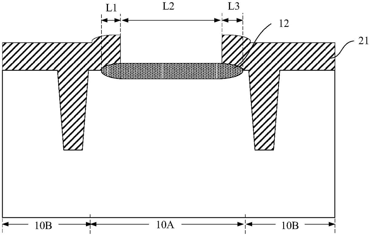
[0037] In order to improve the capacitance Cgc between the gate and the collector, it is usually necessary to form a thicker dielectric layer between the gate electrode and the collector in the redundant cell. figure 1 is a schematic structural diagram of an IGBT device, such as figure 1 As shown, the IGBT device has a plurality of functional cells 10B and a redundant cell 10A between the plurality of functional cells 10B, and the redundant cell 10A includes a collector 11, a dielectric layer 12 and a Gate electrode 13. Wherein, the dielectric layer 12 ...


PUM

PropertyMeasurementUnit
Feature sizeaaaaaaaaaa

Abstract

The invention provides a formation method of an IGBT (Insulated Gate Bipolar Transistor) device, and a structure of an IGBT device. The IGBT device is provided with a plurality of functional cells andredundant cells located between the plurality of functional cells. The formation method of the IGBT device includes the steps: performing an ion implantation process on a semiconductor substrate, ofa first region, for formation of the redundant cells; and performing an oxidation process to form a dielectric layer on the semiconductor substrate of the first region. Therefore, after executing theion implantation process, the oxidation rate of the semiconductor substrate of the first region can be effectively improved, and then the dielectric layer having a higher and more uniform thickness can be formed, and then the capacitance Cgc between a gate and a collector in the IGBT device can be effectively improved. Moreover, the dielectric layer formed by the combination of the ion implantation process and the first oxidation process also has a smaller size, thus reducing the area occupied by the redundant cells, and greatly improving the conduction voltage drop of the IGBT device.

Description

technical field [0001] The invention relates to the technical field of semiconductor manufacturing, in particular to a method for forming an IGBT device and a structure thereof. Background technique [0002] Insulated Gate Bipolar Transistor (IGBT, Insulated Gate Bipolar Transistor) is a new type of high-power device, which combines MOSFET gate voltage control characteristics and low on-resistance characteristics of bipolar transistors, improving device withstand voltage and on-resistance mutual restraint. Among them, IGBT devices generally include planar IGBT devices and trench IGBT devices. For planar IGBT devices, there is a parasitic Junction Field Effect Transistor (JFET) region between each cell. The JFET resistance is an important part of the device resistance and also weakens the conductance modulation effect of the IGBT device. important factor. Therefore, in order to reduce the saturated turn-on voltage drop of the body in the device, the trench structure can be...

Claims


Application Information

Patent Timeline
IPC IPC(8): H01L21/331H01L29/739
CPCH01L29/66325H01L29/7393
Inventor 刘剑
Owner SEMICON MFG INT (SHANGHAI) CORP
Why Eureka
Try Eureka