

An ultraviolet photodiode based on NiO/Ga2O3 and a preparation method thereof
A technology of diodes and ultraviolet light, applied in circuits, electrical components, semiconductor devices, etc., can solve the problems of lack of materials and inability to prepare ultraviolet photodiodes, etc., and achieve excellent detection performance, high critical breakdown electric field strength, and large forbidden band width Effect
- Summary
- Abstract
- Description
- Claims
- Application Information
AI Technical Summary
Problems solved by technology
Method used
Image


Examples
Embodiment 1
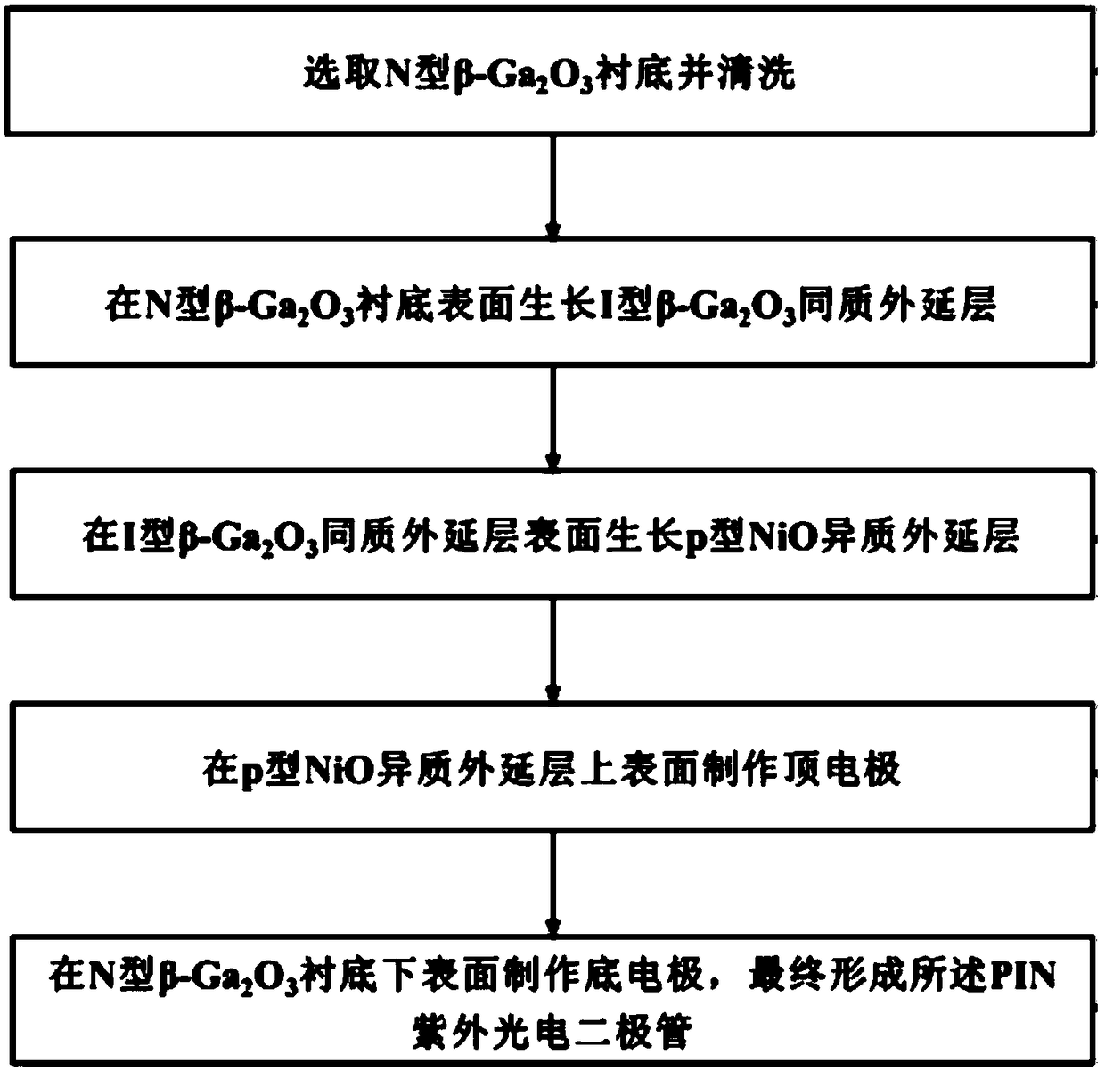
[0040] The present invention is based on NiO / Ga 2 o 3 The preparation method of the UV photodiode, such as figure 2 As shown, the specific steps are as follows:
[0041] Step 1. For N-type single crystal β-Ga 2 o 3 The substrate is cleaned, and after cleaning, it is dried with nitrogen gas for use. The cleaning process is as follows: use cleaning solution-acetone-alcohol-deionized water to clean the sample step by step;
[0042] Step 2, N-type single crystal β-Ga after cleaning in step 1 2 o 3 Intrinsic single crystal β-Ga 2 o 3 Homoepitaxial layer growth, intrinsic single crystal β-Ga 2 o 3 During the growth of the homoepitaxial layer, chemical vapor deposition equipment is used to deposit metal gallium with a purity of 99.99999% as the gallium source, and argon gas is used as the carrier gas. The argon gas flow rate is controlled at 100 ml / min, and the reaction chamber is heated to 800 ° C Introduce oxygen as the growth source gas, the oxygen flow rate is controll...
Embodiment 2
[0047] The present invention is based on NiO / Ga 2 o 3 The preparation method of the UV photodiode, such as figure 2 As shown, the specific steps are as follows:
[0048] Step 1. For N-type single crystal β-Ga 2 o 3 The substrate is cleaned, and after cleaning, it is dried with nitrogen gas for use. The cleaning process is as follows: use cleaning solution-acetone-alcohol-deionized water to clean the sample step by step;
[0049] Step 2, N-type single crystal β-Ga after cleaning in step 1 2 o 3 Intrinsic single crystal β-Ga 2 o 3 Homoepitaxial layer growth, intrinsic single crystal β-Ga 2 o 3 During the growth of the homoepitaxial layer, chemical vapor deposition equipment was used to deposit metal gallium with a purity of 99.99999% as the gallium source, and argon as the carrier gas. The flow rate of the argon gas was controlled at 200 ml / min, and the reaction chamber was heated to 900°C. Introduce oxygen as the growth source gas, control the oxygen flow rate to 5 m...
Embodiment 3
[0054] The present invention is based on NiO / Ga 2 o 3 The preparation method of the UV photodiode, such as figure 2 As shown, the specific steps are as follows:
[0055] Step 1. For N-type single crystal β-Ga 2 o 3 The substrate is cleaned, and after cleaning, it is dried with nitrogen gas for use. The cleaning process is as follows: use cleaning solution-acetone-alcohol-deionized water to clean the sample step by step;
[0056] Step 2, N-type single crystal β-Ga after cleaning in step 1 2 o 3 Intrinsic single crystal β-Ga 2 o 3 Homoepitaxial layer growth, intrinsic single crystal β-Ga 2 o 3 During the growth of the homoepitaxial layer, chemical vapor deposition equipment is used to deposit metal gallium with a purity of 99.99999% as the gallium source, and argon as the carrier gas. The flow rate of the argon gas is controlled at 100 ml / min, and the reaction chamber is heated to 850°C. Introduce oxygen as the growth source gas, the oxygen flow rate is controlled at ...
PUM
| Property | Measurement | Unit |
|---|---|---|
| Doping concentration | aaaaa | aaaaa |
Abstract
Description
Claims
Application Information