Resolution test card for Nano CT imaging quality detection and preparation method of resolution test card

A technology of imaging quality and resolution, which is applied in the field of resolution test chart and its preparation, can solve problems such as unsatisfactory spatial resolution test chart, difficulty in realizing nanoscale, and not too large depth-to-width ratio. The effect of preparation method control and easy preparation method

Active Publication Date: 2018-12-21
INST OF ELECTRICAL ENG CHINESE ACAD OF SCI
View PDF0 Cites 4 Cited by
  • Summary
  • Abstract
  • Description
  • Claims
  • Application Information

AI Technical Summary

Problems solved by technology

Micromachining can only achieve micron details by mechanical means; the size of LIGA processing can reach the micro-nano scale, but the cost of LIGA processing is relatively high; ion beam processing can reach the micro-nano scale, but the aspect ratio cannot be too large; laser The processing speed is fast and the precision is high, but it is difficult to achieve nanoscale
At present, the spatial resolution test cards of X-ray imaging in the market are provided by foreign companies such as German QRM Company, American Phantomlab Company and JIMA (Japan Inspection Instrument

Method used


Image

  • Resolution test card for Nano CT imaging quality detection and preparation method of resolution test card
  • Resolution test card for Nano CT imaging quality detection and preparation method of resolution test card

Examples


preparation example Construction

[0019] The invention provides a method for preparing a resolution test card for Nano CT imaging quality detection, which specifically includes the following steps:

[0020] Step 1. Pretreat the substrate 1 used to prepare the resolution test card, and obtain the pretreated substrate 1;

[0021] The pretreatment is as follows: firstly, the tungsten block is processed into a circular thin tungsten sheet with a diameter of 3-10 mm and a thickness of 200 μm by mechanical processing; then the circular thin tungsten sheet is mechanically polished, and ionized Thinner thins the thickness of the circular thin tungsten sheet after mechanical polishing to 1-5 μm; then uses industrial ethanol to perform ultrasonic cleaning on the thinned circular thin tungsten sheet, and the ultrasonic cleaning time is 5-10 minutes; Finally, the cleaned circular thin tungsten sheet is placed in a drying dish for drying to obtain the pretreated substrate 1;

[0022] Step 2. Place the pretreated substrate...

Embodiment 1

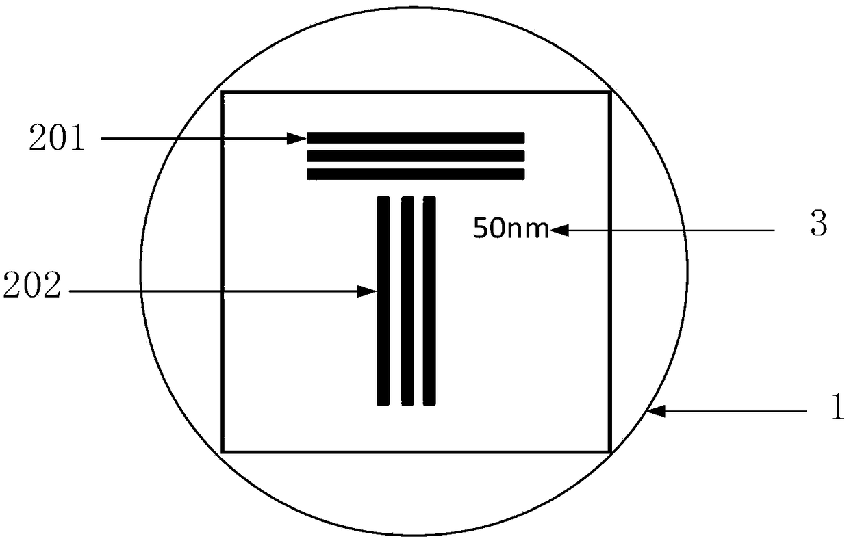
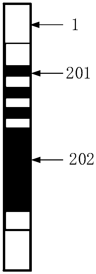
[0031] Such as figure 1 and figure 2 As shown, a resolution test card for Nano-CT imaging quality provided by the present invention includes a substrate 1 , horizontal stripes 201 , vertical stripes 202 and a scale 3 . The base 1 is preferably a circular thin tungsten sheet with a diameter of 3 mm and a thickness of 1 μm. The horizontal stripes 201 and the vertical stripes 202 are both rectangular parallelepiped, each has 3 stripes, each horizontal stripe 201 and each vertical stripe 202 have an etching width of 50 nm, an etching length of 3 μm, and an etching depth of 1 μm The overall horizontal stripes 201 and the vertical stripes 202 are distributed in a T shape on the substrate, and the horizontal stripes 201 and the vertical stripes 202 are etched by gallium ion beams emitted by a gallium ion source in a helium ion microscope. The helium The working condition of the gallium ion beam of the ion microscope is that the accelerating voltage is 25kV, the beam current is 10p...

Embodiment 2

[0040] Another resolution test card for Nano-CT imaging quality provided by the present invention includes a substrate 1 , horizontal stripes 201 , vertical stripes 202 and a scale 3 . The base 1 is preferably a circular thin tungsten sheet with a diameter of 10 mm and a thickness of 5 μm. The horizontal stripes 201 and the vertical stripes 202 are both cuboids, each having 5 stripes, each of the horizontal stripes 201 and the vertical stripes 202 has an etching width of 1 μm, an etching length of 5 μm, and an etching depth of 5 μm. The stripes 201 and the vertical stripes 202 are distributed in a T shape, and the horizontal stripes 201 and the vertical stripes 202 are etched by the gallium ion beam emitted by the gallium ion source in the helium ion microscope. The working conditions of the gallium ion beam of the helium ion microscope are The acceleration voltage is 30kV, the beam current is 15pA, and the duty ratio of the acceleration voltage is 1:1. The scale 3 uses the ga...


PUM

PropertyMeasurementUnit
Diameteraaaaaaaaaa
Thicknessaaaaaaaaaa
Widthaaaaaaaaaa

Abstract

The invention discloses a preparation method of a resolution test card for Nano CT imaging quality detection and belongs to the technical fields of nanometer materials and CT imaging. The method comprises the steps that a base body is preprocessed, and the preprocessed base body is acquired; the preprocessed base body is placed on a sample table inside a helium ion microscope, a gallium ion beam current generated by a gallium ion source in the helium ion microscope is utilized to perform etching on the preprocessed base body, and etched stripes are acquired; and width calibration is performedon the etched stripes, and the resolution test card is acquired. The invention furthermore provides the resolution test card prepared through the method for Nano CT imaging quality detection. The preparation method has the advantages that control is easy, the process is simple, the cycle is short, efficiency is high, and cost is low; and the prepared resolution test card for Nano-CT imaging quality detection is uniform in stripe width and large in depth ratio.

Description

technical field [0001] The invention belongs to the technical field of nanomaterials and CT imaging, and relates to a resolution test card for quality detection of Nano CT imaging and a preparation method thereof. Background technique [0002] Nano CT is a new imaging device with higher resolution developed on the basis of Micro CT, which improves the spatial resolution of X-ray imaging to the nanometer level, and is widely used in many fields such as biological imaging, pathological detection and integrated circuit detection. There are broad application prospects. The imaging quality of Nano CT generally uses a resolution test card, which can objectively describe the image resolution, and intuitively and simply reflect the image resolution performance index. However, with the improvement of the resolution of Nano CT, the processing of the resolution test chart is difficult and costly, especially when the system resolution is high, it is difficult to realize the ideal point...

Claims


Application Information

Patent Timeline
IPC IPC(8): G01N23/046
CPCG01N23/046
Inventor 马玉田刘俊标韩立
Owner INST OF ELECTRICAL ENG CHINESE ACAD OF SCI
Why Eureka
Try Eureka