Organic semiconductor material and luminescent device

A technology of organic semiconductors and matrix materials, applied in semiconductor devices, semiconductor/solid-state device manufacturing, electric solid-state devices, etc., can solve problems such as the lack of auxiliary semiconductor materials, and achieve the effect of reducing turn-on voltage and improving efficiency

Inactive Publication Date: 2018-12-25
AAC TECH NANJING
View PDF14 Cites 14 Cited by
  • Summary
  • Abstract
  • Description
  • Claims
  • Application Information

AI Technical Summary

Problems solved by technology

[0014] However, for high-energy light-emitting systems, especially deep blue light-emitting material systems, the corresponding auxiliary semiconductor materials for improving electrical properties are lacking.

Method used


Image

  • Organic semiconductor material and luminescent device
  • Organic semiconductor material and luminescent device
  • Organic semiconductor material and luminescent device

Examples


preparation example Construction

[0090] Preparation of organic semiconductor materials:

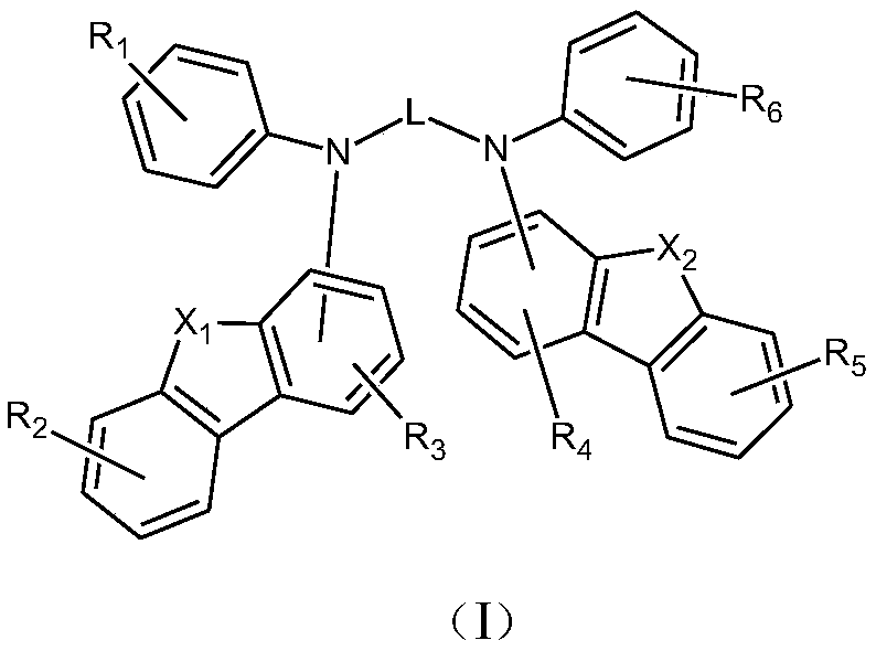
[0091] Method A: general synthetic route of general formula (I)

[0092] The method for preparing the compound of dibenzofuran structure, mixing dibenzofuran boronic acid and brominated aromatic compound in tetrahydrofuran, adding sodium carbonate and catalyst palladium acetate, heating and reacting for 24 hours, cooling, and extracting with dichloromethane, the column layer analysis and purification to obtain aryl-substituted dibenzofuran, and then react the obtained aryl-substituted dibenzofuran with liquid bromine in the presence of butyllithium in low-temperature tetrahydrofuran for 12 hours, and post-treatment to obtain bromine-substituted dibenzofuran. Benzofuran compound, finally react bromine-substituted dibenzofuran compound with corresponding amine in palladium acetate, ligand tri-tert-butylphosphine tBu3P, base tBuONa for 24h in dry toluene, extract with dichloromethane after cooling , column chromatography p...

Embodiment 1

[0100] The synthesis of embodiment 1:S001

[0101]

[0102] Bromobenzene (10.0mmol), dibenzofuran-4-boronic acid (12.0mmol), palladium acetate (0.3mmol) and sodium carbonate (20.00mmol) were dissolved in 50mL of tetrahydrofuran, reacted at 65°C for 24 hours, cooled, added water and Dichloromethane, the organic layer was concentrated and column chromatographed to obtain an intermediate product (S001-3). S001-3 (5mmol), liquid bromine (6mmol), and butyllithium (5mmol) were dissolved in 30mL of tetrahydrofuran, reacted at -78°C for 12h, and worked up to obtain the intermediate product S001-4. Dissolve 2,6-dibromospirobifluorene (10mmol) and aniline (20mmol) in 100mL of dry toluene, add catalyst palladium acetate, ligand tBu3P, base tBuONa, react under nitrogen for 12h, cool with dichloro Methane extraction. Then column chromatography gave the intermediate product S001-7. Dissolve S001-4 (5mmol) and S001-7 (5mmol) in 50mL dry toluene, add palladium acetate, ligand tBu3P, base ...

Embodiment 2

[0103] Embodiment 2: the synthesis of S002

[0104]

[0105] Dissolve 2,6-dibromospirobifluorene (10mmol) and 4-aminobiphenyl (20mmol) in 100mL dry toluene, add catalyst palladium acetate, ligand tBu3P, base tBuONa, react under nitrogen for 12h, cool Then extract with dichloromethane. Then column chromatography gave the intermediate product S002-7. Dissolve S001-4 (5mmol) and S002-7 (5mmol) in 50mL dry toluene, add palladium acetate, ligand tBu3P, base tBuONa, react for 12h under nitrogen, extract with dichloromethane after cooling, and obtain after column chromatography Final product S002 (2.3 mmol), yield 46.0%. MS (ESI-TOF): The measured mass-to-nucleus ratio m / z is 1135.35 [M+].


PUM

PropertyMeasurementUnit
thicknessaaaaaaaaaa
thicknessaaaaaaaaaa
thicknessaaaaaaaaaa

Abstract

The invention belongs to the technical field of electroluminescent materials, and discloses an organic semiconductor material and a luminescent device. The organic semiconductor material comprises atleast one substrate material and at least one doping material. The substrate materials are provided with structures shown as a general formula (I), and the doping materials are provided with structures shown as a general formula (II) or a general formula (III). The organic semiconductor material and the luminescent device have the advantages that lightening voltages of the luminescent device prepared from the organic semiconductor material can be obviously lowered, and the luminescent efficiency of the luminescent device can be obviously improved; the efficiency of the organic semiconductor material for deep blue phosphorescent devices can be obviously improved, and accordingly application of the organic semiconductor material to sky blue phosphorescent devices, green phosphorescent devices and red phosphorescent devices can be anticipated according to energy transfer principles.

Description

technical field [0001] The invention belongs to the technical field of electroluminescent materials, and in particular relates to an organic semiconductor material and a light emitting device. Background technique [0002] The use of organic materials to prepare various functional devices, especially for photoelectrically responsive functional devices, such as common organic electroluminescent devices, organic solar cell devices, organic field effect transistor devices and organic photosensitive sensor devices, has attracted more and more attention. . [0003] Organic electroluminescent device is a device technology that realizes electroluminescence by introducing one or more layers of organic films on the cathode and anode. It can achieve ultra-thin, flexible and transparent performance, and is used in flat panel display and lighting industries. increase year by year. [0004] The structure of organic electroluminescent devices in the industry can be realized by different...

Claims


Application Information

Patent Timeline
Patent Type & Authority Applications(China)
IPC IPC(8): C07C255/51C07C261/02C07C265/12C07C331/08C07D213/61C07D307/91C07D405/14H01L51/00H01L51/54
CPCC07C255/51C07C261/02C07C265/12C07C331/08C07D213/61C07D307/91C07D405/14C07C2601/02H10K85/60H10K85/624H10K85/636H10K85/633H10K85/615H10K85/654H10K85/6574
Inventor 黄达曹辰辉孙晓媛马腾达陈少海
Owner AAC TECH NANJING
Why Eureka
Try Eureka