
A high-precision micro-stress sensor

A micro-stress and sensor technology, applied in instruments, measuring force, and force measurement by measuring the change of optical properties of materials under stress, etc. , to achieve the effect of small phase detection error, wide application occasions, and improved sensing accuracy

Inactive Publication Date: 2019-11-19
JILIN UNIV
View PDF1 Cites 0 Cited by
  • Summary
  • Abstract
  • Description
  • Claims
  • Application Information

AI Technical Summary

Problems solved by technology

However, on the one hand, the high-frequency component itself will affect the phase detection of the cosine wave (the position of the zero-crossing point changes); The electrical characteristics are equivalent to capacitance, and the voltage at both ends cannot jump, so the falling edge of the sawtooth wave cannot be infinitely short) and the elasticity of the optical fiber itself and many other factors, the frequency is variable, and it is difficult to filter out cleanly; and , when using a filter, in addition to affecting the amplitude-frequency characteristics of the output signal, it will also affect the phase-frequency characteristics of the signal at the same time, that is, the phase of the filter will be affected near the cut-off frequency, which is very important for relying on phase changes. It is very disadvantageous for fiber optic sensors that measure changes in stress

Method used


Image

  • A high-precision micro-stress sensor
  • A high-precision micro-stress sensor
  • A high-precision micro-stress sensor

Examples


Embodiment 1

[0026] Embodiment 1 Overall structure of the present invention

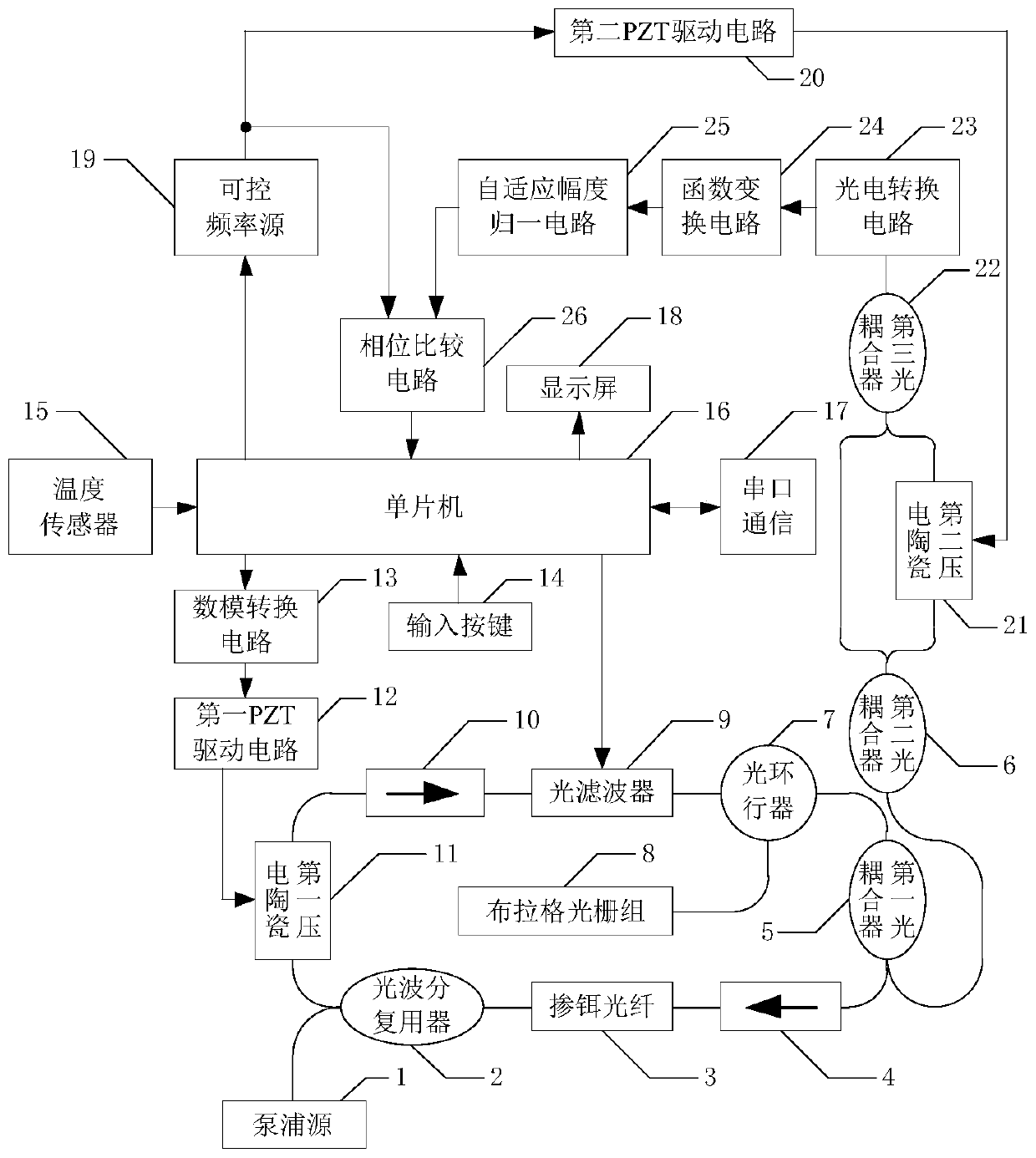
[0027] Such as figure 1 Shown, the overall structure of the present invention has, pump source 1 (the LC962U type pump source of OCLARO Company, central wavelength 980nm, the maximum single-mode output optical power is 750mW) and optical wavelength division multiplexer 2 (COMCORE Company 980 / 1060nm The 980nm end of the single-mode optical fiber wavelength division multiplexer) is connected, and the 1550nm end of the optical wavelength division multiplexer 2 is wound on the first piezoelectric ceramic 11 (cylindrical piezoelectric ceramic, outer diameter 50mm, inner diameter 40mm, height 50mm) One end of the optical fiber is connected, the other end of the optical fiber wound on the first piezoelectric ceramic 11 is connected to the input end of the first optical isolator 10 (THORLABS company IO-H-1064B single-mode optical isolator), the first piezoelectric The control terminal of the ceramic 11 is connected to t...

Embodiment 2

[0029] Embodiment 2 function transformation circuit

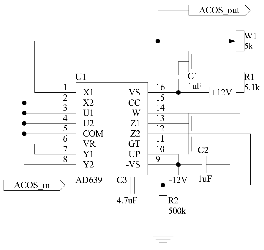
[0030] The structure of the function conversion circuit 24 is as follows: one end of the capacitor C3 is connected to the pin 12 of the trigonometric function converter U1 and one end of the resistor R2, and the other end of the capacitor C3 is used as the input terminal of the function conversion circuit 24, which is recorded as the port ACOS_in , connected to the output end of the photoelectric conversion circuit 23; the other end of the resistor R2 is grounded; the pins 2, 3, 4, 5, 8, 11, 13 of the trigonometric function converter U1 are grounded, and the pins 9, 10 are connected to the capacitor C2 One end is connected to -12V power supply, the other end of capacitor C2 is grounded; pin 6 of trigonometric function converter U1 is connected to pin 7, pin 16 is connected to +12V power supply and one end of capacitor C1, and the other end of capacitor C1 is grounded; The pin 1 of the trigonometric function converter U1 is ...

Embodiment 3

[0031] Embodiment 3 Adaptive Amplitude Normalization Circuit

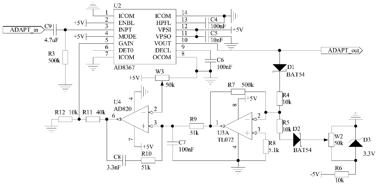
[0032]Because the amplitude of the signal output by the function conversion circuit 24 is small, and is affected by multiple parameters in the optical path and the circuit, the size is indefinite, so the present invention designs an adaptive amplitude normalization circuit 25, which is used to convert the signal output by the function conversion circuit 24 The amplitude is normalized to the optimal size to further improve the accuracy of demodulation. The structure of the adaptive amplitude normalization circuit 25 is that one end of the capacitor C9 is connected to one end of the resistor R3 and the pin 3 of the chip U2, the other end of the resistor R3 is grounded, and the other end of the capacitor C9 is used as an adaptive amplitude normalization The input end of the circuit 25 is recorded as the port ADAPT_in, which is connected with the port ACOS_out of the function transformation circuit 24; the pin 1, the p...


PUM

PropertyMeasurementUnit
wavelengthaaaaaaaaaa
reflectanceaaaaaaaaaa

Abstract

The invention discloses a highly precise micro-stress sensor, and belongs to the technical field of optical fiber sensors. The main structure of the micro-stress sensor comprises a pump source (1), anoptical wavelength division multiplexer (2), an erbium doped fiber (3), and the like. According to the highly precise micro-stress sensor a sinusoidal signal is used as a modulation signal, high-frequency interference is not generated, and the micro-stress sensor has the characteristics of being more reliable in operation, high in sensing precision, wide in application range, and the like.

Description

technical field [0001] The invention belongs to the technical field of optical fiber sensors, in particular to a high-precision micro-stress sensor. Background technique [0002] Fiber Bragg grating (FBG) is widely used in the field of sensing technology due to its advantages of anti-electromagnetic interference, chemical resistance, small transmission loss, small size and light weight, and easy mass production. At present, stress sensors are widely used in the field of engineering technology. Especially in emerging fields such as nanoparticle interaction and cell mechanics, there is an urgent need for micro-stress sensors, and the safety monitoring of bridges, tunnels, and building structures is inseparable from micro-stress sensors. Due to the above-mentioned advantages of the fiber Bragg grating, the stress sensor formed by it has higher reliability than other sensors, and is more suitable for use under harsh conditions. [0003] The prior art closest to the present inv...

Claims


Application Information

Patent Timeline
Patent Type & Authority Patents(China)
IPC IPC(8): G01L1/24
CPCG01L1/246
Inventor 高博林旻霍佳雨钟思源邱天张栋
Owner JILIN UNIV
Learn More