A thermally induced voltage material and application thereof
An induced voltage and electrode technology, applied in the field of lateral thermoelectric materials and devices, can solve the problems of large detection element dimensions, difficulty in capturing thermal field, slow response speed, etc., and achieve large measurement dynamic range, simple workflow, heat capacity and heat Small effect
- Summary
- Abstract
- Description
- Claims
- Application Information
AI Technical Summary
Problems solved by technology
Method used
Image
Examples
Embodiment 1
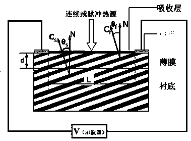
[0016] exist figure 1 Na x CoO 2 Thin film, where x=0.6 is used as thermally induced voltage material; firstly, the SrTiO 3 Growth of (Ca / Na) with a thickness of 200 nm on a single crystal substrate 0.6 CoO 2 film; then two electrodes are prepared at a distance of 3 mm in the inclined direction of the film surface, and the leads at both ends of the electrodes are connected to the coaxial cable, and a high-frequency oscilloscope is connected according to Figure 1; the surface of the film is irradiated with a xenon lamp, The voltage signal mV is obtained on the surface, and the signal response rate is 0.54mV / W / cm 2 .
Embodiment 2
[0018] exist figure 1 Na 0.7 CoO 2 Thin film, as a thermally induced voltage material; firstly, the α-Al 2 o 3 Na with a thickness of 100 nm was grown on a single crystal substrate 0.7 CoO 2 film; then prepare two electrodes at an interval of 4 mm in the inclined direction of the film surface, connect leads to the coaxial cable at both ends of the electrodes, and connect a high-frequency oscilloscope according to Figure 1; irradiate the surface of the film with a xenon lamp, The voltage signal mV is obtained on the surface, and the signal response rate is 0.72mV / W / cm 2 .
Embodiment 3
[0020] exist figure 1 Ca 0.5 CoO 2 thin film, as a thermally induced voltage material; firstly, LaAlO with an inclination angle of 5° was deposited by pulsed laser deposition 3 Growth of Ca with a thickness of 500 nm on a single crystal substrate 0.5 CoO 2 film; then prepare two electrodes at an interval of 4 mm in the inclined direction of the film surface, connect leads to the coaxial cable at both ends of the electrodes, and connect a high-frequency oscilloscope according to Figure 1; irradiate the surface of the film with a xenon lamp, The voltage signal mV is obtained on the surface, and the signal response rate is 0.58mV / W / cm 2 .
PUM
 Abstract
Description
Claims
Application Information
