
Eureka
For R&D, Eureka makes reading and utilizing patents & technical documents easy.
Eureka AIR
Designed for self-driven R&D workflows. Generate viable solutions, solve complex R&D challenges, empower your innovation with AI.

Eureka Materials
Designed for material experts only. Revolutionize your material R&D, from search, analyze, to developing new materials.

TechResearch
Generate reliable direction feasibility study reports for your R&D in just a few steps.

TechSeek
Discover and master advanced knowledge NOW. Basics, ideas, possibilities, all at once.

TechMind
As an expert in R&D Theories, TechMind can generates customized viable solutions instantly.

TechRisk
Analyze your overall solution with one click, know your potential R&D risks in advance.

TechMonitor
Get weekly tech updates, stay abreast of the latest tech innovations and key insights.
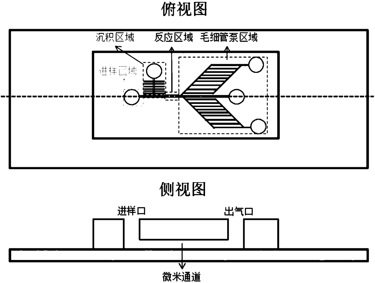
Protein detecting chip based on micro-nanometer fluid and preparation method of protein detecting chip
A protein detection and micro-nanofluid technology, applied in the biological field, can solve the problems of slow detection speed, complex operation, low sensitivity, etc., and achieve the effect of reducing chip cost, high detection sensitivity, and fast and high-sensitivity detection.
- Summary
- Abstract
- Description
- Claims
- Application Information
AI Technical Summary
Problems solved by technology
Method used
Image

Examples
Embodiment 1
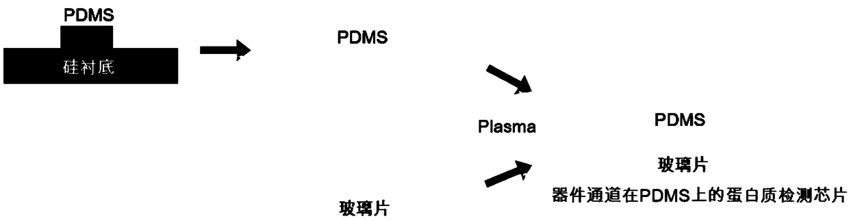
[0026] Preparation of protein detection chip with device channel on PDMS
[0027] Firstly, a SU8 silicon wafer template with a thickness of 20-200 μm is prepared on the silicon wafer by photolithography of the SU8 photoresist on the front side. Mix and stir 30 g of PDMS solution with A / B=1 / 10 evenly, then vacuumize to remove air bubbles. Then add the clear PDMS mixture on the surface of the SU8 silicon wafer template and cure at 80°C for 1h. Gently tear off the PDMS and cut and separate the PDMS containing individual devices with a knife. Clean the PDMS with each device. The process is to ultrasonically clean with acetone for 5 minutes, then with isopropanol for 5 minutes, and then with DIwater for 5 minutes. 2 Air dry. The clean PDMS with devices and the glass slide were punched under 60W plasma for 60s and bonded together immediately to obtain a protein detection chip with device channels on PDMS.
Embodiment 2
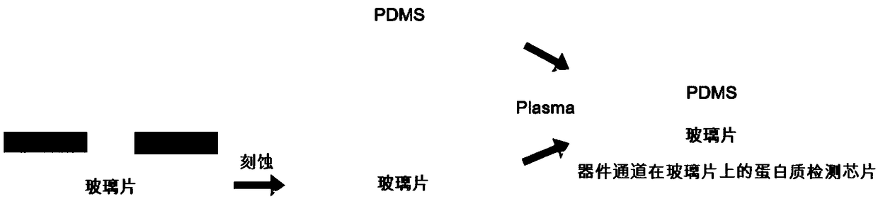
[0029] Preparation of protein detection chips with device channels on glass slides
[0030] Firstly, a glass plate template with a photoresist thickness of 1-10 μm is prepared on the glass plate by front photolithography. Then immerse the template in BOE (6:1) solution wet etching for 3-6h, or use dry etching on the template, so that the thickness of each channel on the glass sheet is 20-200 μm. Cut and separate the components on the glass slide and clean them. The clean glass slide with device and the flat PDMS substrate were punched under 60W plasma for 60s and bonded together immediately to obtain a protein detection chip with the device channel on the glass slide.
Embodiment 3
[0032] Fabrication of a protein detection chip with integrated gold nanorods in the reaction area
[0033] Gold nanorods were grown on glass slides by oblique angle deposition (OAD). The normal direction of the glass substrate forms an angle θ with the vapor direction (evaporation angle). The gun filament under the device emits an electron beam under high pressure to evaporate the raw material source (gold, silver, silicon dioxide, etc.) in the crucible.
[0034]Vapor nucleates first on the substrate surface, and nucleation centers on these surfaces continue to grow into nanostructures due to limited surface atom diffusion and shadowing effects. The shape parameters of the nanostructure can be controlled by controlling the evaporation angle θ, the rotation speed of the substrate during deposition, the deposition thickness, the deposition rate, and the power, and the maximum fluorescence enhancement effect can be achieved through optimization. In this embodiment, during the m...
PUM
| Property | Measurement | Unit |
|---|---|---|
| Diameter | aaaaa | aaaaa |
| Thickness | aaaaa | aaaaa |
| Spacing | aaaaa | aaaaa |
Abstract
Description
Claims
Application Information
 - R&D Engineer
- R&D Manager
- IP Professional
- Industry Leading Data Capabilities
- Powerful AI technology
- Patent DNA Extraction
Browse by: Latest US Patents, China's latest patents, Technical Efficacy Thesaurus, Application Domain, Technology Topic, Popular Technical Reports.
© 2024 PatSnap. All rights reserved.Legal|Privacy policy|Modern Slavery Act Transparency Statement|Sitemap|About US| Contact US: help@patsnap.com