AlGaN-based ultraviolet LED structure grown on Si substrate by PLD combined with MOCVD method and preparation method thereof
A LED structure and substrate technology, applied in semiconductor/solid-state device manufacturing, electrical components, circuits, etc., can solve the problems of low luminous efficiency, rough surface, and low Al atom migration ability of ultraviolet LEDs
- Summary
- Abstract
- Description
- Claims
- Application Information
AI Technical Summary
Problems solved by technology
Method used
Image

Examples
preparation example Construction
[0041] The method for preparing an AlGaN-based ultraviolet LED structure grown on a Si substrate by combining the PLD with the MOCVD method includes the following steps:
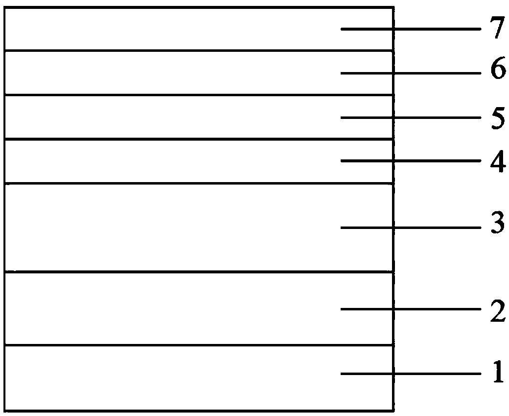
[0042] Preparation of stepping AlGaN buffer layer: grow stepping AlGaN buffer layer on Si(111) substrate by pulsed laser deposition method, growth temperature is 600-700°C, laser energy is 200-250mJ, laser frequency is 5-30Hz, air pressure 1-30mTorr, the number of layers is 1-3, the Al composition changes from 0-0.8, and the total thickness of the film is 200-800nm; preferably, the conditions of the pulsed laser deposition method are that the growth temperature is 650-680°C, and the laser energy is 220 -230mJ, laser frequency 10-20Hz, air pressure 8-25mTorr.
[0043] Preparation of Si-doped n-type AlGaN layer: The n-type doped AlGaN layer is grown on the stepping AlGaN buffer layer by metal-organic vapor deposition method, the growth temperature is 1000-1100 °C, and the Si doping concentration is 5×10 20 -7...
Embodiment 1
[0050] A high-quality AlGaN-based deep ultraviolet LED structure epitaxially grown on a Si(111) substrate, the preparation method of the deep ultraviolet LED structure comprises the following steps:
[0051]1) Preparation of a stepping AlGaN buffer layer: a stepping AlGaN buffer layer is grown on a Si(111) substrate using PLD technology, the growth temperature is 600°C, the laser energy is 220mJ, the laser frequency is 15Hz, the gas pressure is 15mTorr, and the number of layers is 1. The Al component is 0, and the total thickness of the film is 200nm;
[0052] 2) Preparation of Si-doped n-type AlGaN layer: On the stepped AlGaN buffer layer, a Si-doped n-type doped AlGaN layer was grown by MOCVD technology, the growth temperature was 1000°C, and the Si doping concentration was 5× 10 20 cm -3 , the film thickness is 2500nm;
[0053] 3)Al 0.40 Ga 0.60 N / Al 0.50 Ga 0.50 Preparation of N multi-quantum well layer: growing Al on the n-type doped AlGaN layer by MOCVD technology...
Embodiment 2
[0058] A high-quality AlGaN-based deep ultraviolet LED structure epitaxially grown on a Si(111) substrate, the preparation method of the deep ultraviolet LED structure comprises the following steps:
[0059] 1) Preparation of a stepping AlGaN buffer layer: a stepping AlGaN buffer layer is grown on a Si(111) substrate using PLD technology, the growth temperature is 600°C, the laser energy is 220mJ, the laser frequency is 15Hz, the gas pressure is 15mTorr, and the number of layers is 3. The AL components of each layer from bottom to top are 0, 0.28 and 0.64, and the thickness of each layer is 200, 150 and 450nm;
[0060] 2) Preparation of Si-doped n-type AlGaN layer: grow Si-doped n-type AlGaN layer on the stepped AlGaN buffer layer by MOCVD technology, the growth temperature is 1100°C, and the doping concentration is 7×10 20 cm -3 , the film thickness is 3500nm;
[0061] 3)Al 0.40 Ga 0.60 N / Al 0.50 Ga 0.50 Preparation of N multiquantum well layer: growing Al on Si-doped n...
PUM
| Property | Measurement | Unit |
|---|---|---|
| Thickness | aaaaa | aaaaa |
| Thickness | aaaaa | aaaaa |
| Thickness | aaaaa | aaaaa |
Abstract
Description
Claims
Application Information
 - R&D
- Intellectual Property
- Life Sciences
- Materials
- Tech Scout
- Unparalleled Data Quality
- Higher Quality Content
- 60% Fewer Hallucinations
Browse by: Latest US Patents, China's latest patents, Technical Efficacy Thesaurus, Application Domain, Technology Topic, Popular Technical Reports.
© 2025 PatSnap. All rights reserved.Legal|Privacy policy|Modern Slavery Act Transparency Statement|Sitemap|About US| Contact US: help@patsnap.com