

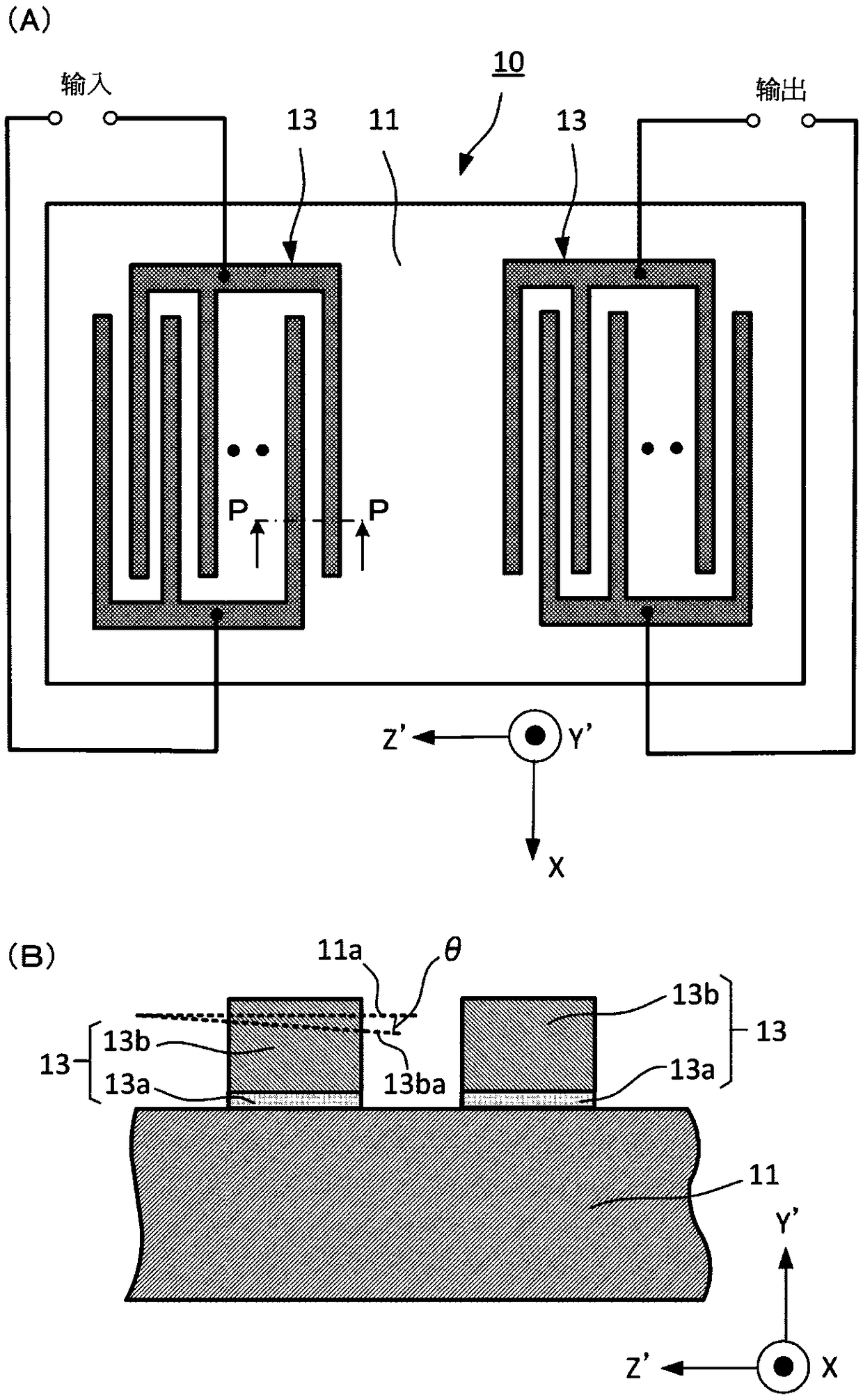
Surface acoustic wave device and method for manufacturing the same
A technology of surface acoustic wave and manufacturing method, which is applied in the manufacturing/assembly of electrical components, piezoelectric/electrostrictive devices, chemical instruments and methods, etc., can solve the problems of electrical resistance deterioration of filters and the like
- Summary
- Abstract
- Description
- Claims
- Application Information
AI Technical Summary
Problems solved by technology
Method used
Image

Examples
Embodiment 2
[0092] As Example 2, the piezoelectric single crystal substrate is set to 36 degrees Y-cut LiTaO 3 Examples of substrates are described. Ready as 36 degree Y-cut LiTaO 3 The main surface of the substrate is ground to a polished surface by mechanical polishing. The substrate was ultrasonically cleaned with pure water in the same manner as in Example 1, then introduced into a DC magnetron sputtering apparatus, and a titanium film and an Al-0.5Cu film were sequentially laminated. Here, the film forming rate of the titanium film was fixed at 0.23 nm / sec and the thickness of the Ti film was varied within the range of 2 nm to 50 nm. The film thickness of the Al-0.5Cu film is the same as in Example 1. In addition, the film formation rate was obtained by setting the film formation conditions of the titanium film as an argon flow rate of 50 sccm and a DC power of 300W. The substrate temperature was set to room temperature in the same manner as in Example 1.
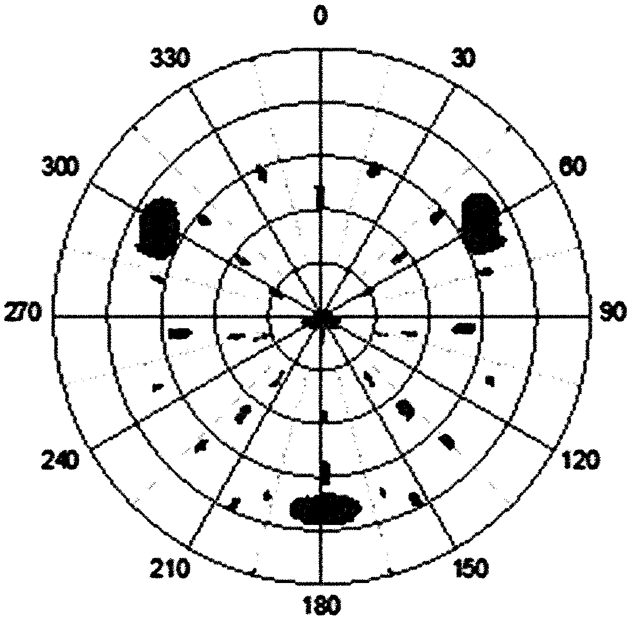
[0093] About the prod...
Embodiment 3
[0099] As Example 3, the piezoelectric single crystal substrate is set to 50 degrees Y-cut LiTaO 3 Examples of substrates are described. Ready as 50 degree Y-cut LiTaO 3 The main surface of the substrate is ground to a polished surface by mechanical polishing. The substrate was ultrasonically cleaned with pure water in the same manner as in Example 1, then introduced into a DC magnetron sputtering apparatus, and a titanium film and an Al-0.5Cu film were sequentially laminated. Here, the film forming rate of the titanium film was fixed at 0.50 nm / sec and the thickness of the Ti film was varied within the range of 5 nm to 50 nm. The film thickness of the Al-0.5Cu film is the same as in Example 1. In addition, the film formation rate was obtained by setting the film formation conditions of the titanium film as an argon flow rate of 50 sccm and a DC power of 500 W. The substrate temperature was set to room temperature in the same manner as in Example 1.
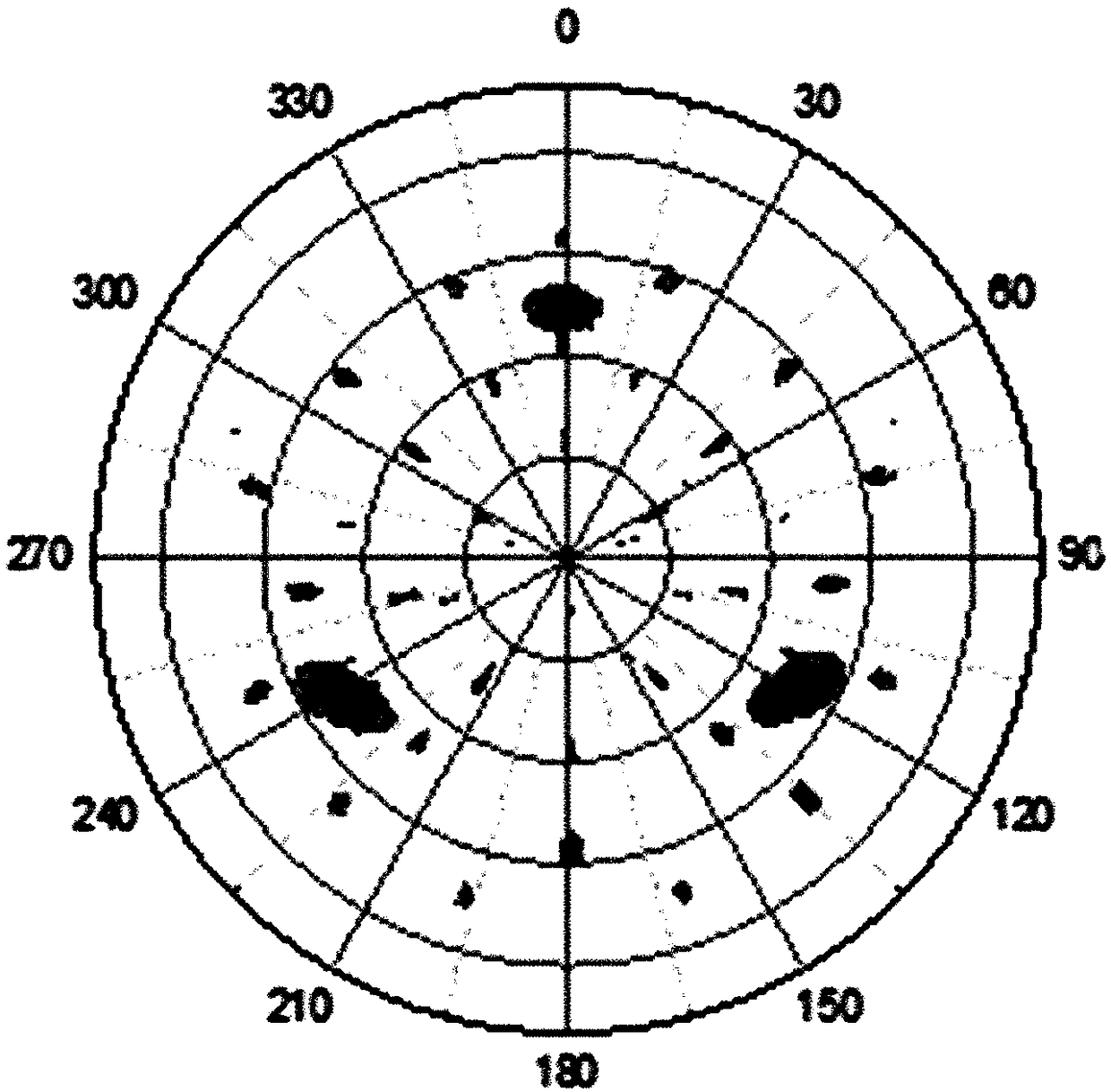
[0100] About the pro...
PUM
| Property | Measurement | Unit |
|---|---|---|
| thickness | aaaaa | aaaaa |
| particle size | aaaaa | aaaaa |
| thickness | aaaaa | aaaaa |
Abstract
Description
Claims
Application Information