

Method of electron beam/ion beam focused etching and microscopic imaging on non-conductive substrate
A technology of ion beam focusing and microscopic imaging, which is applied in the direction of microstructure technology, microstructure devices, manufacturing microstructure devices, etc. It can solve problems such as blurred imaging, failure to meet requirements, interference with electron beam/ion beam focusing effects, etc.
- Summary
- Abstract
- Description
- Claims
- Application Information
AI Technical Summary
Problems solved by technology
Method used
Image


Examples
Embodiment
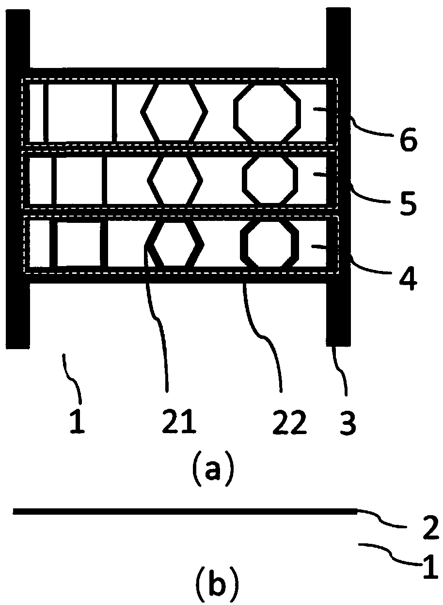
[0032] In this embodiment, the method for performing electron beam / ion beam focused etching and microscopic imaging on a non-conductive substrate includes the following steps:
[0033] S1 Design the shape and size of the photolithography mask;
[0034] S2 performing photolithographic treatment on the non-conductive substrate;
[0035] S3 performing metal coating treatment on the photolithographically processed non-conductive substrate to form a metal strip;
[0036] S4 develops the coated non-conductive substrate to become a sample;
[0037] S5 conducts grounding treatment on the metal belt;
[0038] S6 vacuumizes the sample;
[0039] S7 focuses on the metal strip of the sample, selects the electron beam current, and adjusts the sample stage to the sample area to be engraved after the imaging is clear;
[0040] S8 imports or draws the morphology of the micro-nano structure to be etched, and performs FIB or EBL etching and imaging on the sample after setting parameters.
...
PUM
| Property | Measurement | Unit |
|---|---|---|
| Thickness | aaaaa | aaaaa |
| Thickness | aaaaa | aaaaa |
Abstract
Description
Claims
Application Information