Semiconductor structure and forming method thereof

A technology of semiconductor and gate structure, applied in the field of semiconductor structure and its formation, can solve problems such as different contact resistance effects

Active Publication Date: 2019-01-15
SEMICONDUCTOR MANUFACTURING INTERNATIONAL (BEIJING) CORP +1
View PDF6 Cites 1 Cited by
  • Summary
  • Abstract
  • Description
  • Claims
  • Application Information

AI Technical Summary

Problems solved by technology

[0004] At present, for the PMOS (Metal Oxide Semiconductor) area and the NMOS area, the metal silicide material used is the same, but the effect of the metal silicide on reducing the contact resistance of the PMOS area and the NMOS area is different.

Method used


Image

  • Semiconductor structure and forming method thereof
  • Semiconductor structure and forming method thereof
  • Semiconductor structure and forming method thereof

Examples


Embodiment Construction

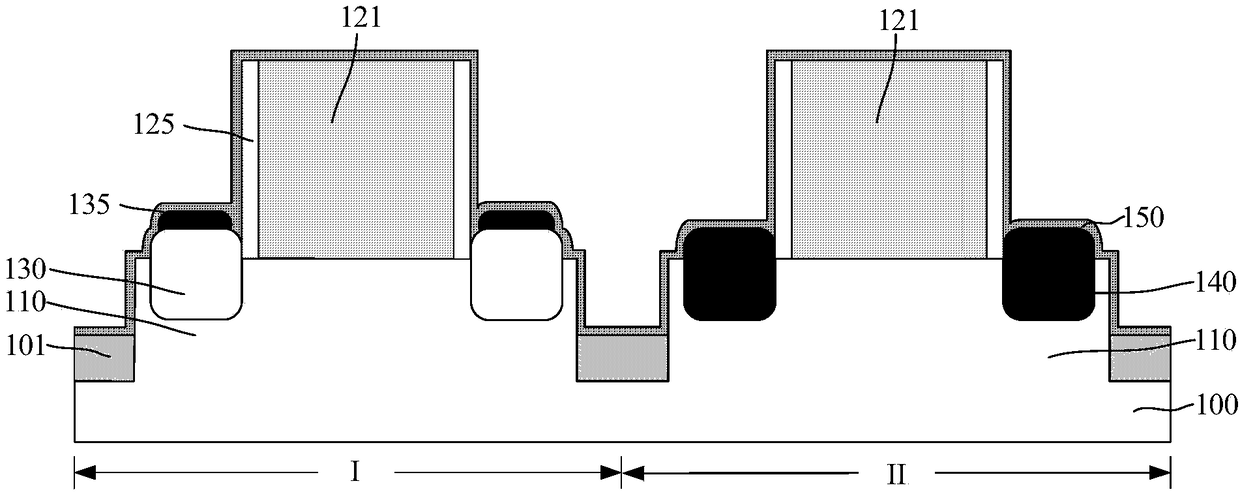
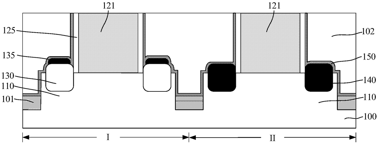
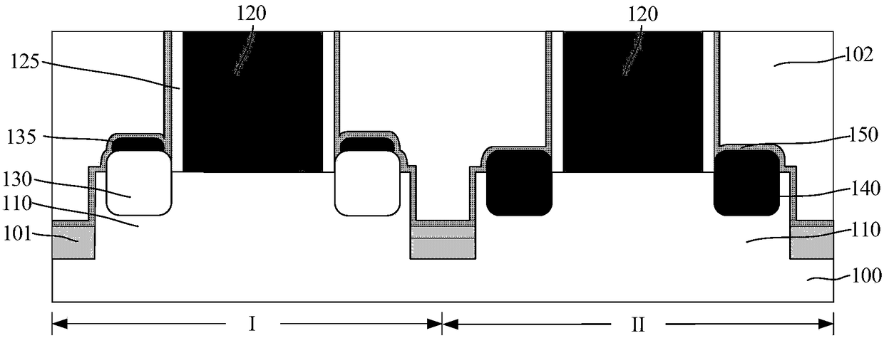
[0033] It is known from the background technology that the contact resistance of the PMOS region needs to be reduced.

[0034] During the formation of the semiconductor structure, the metal silicide layer is usually formed by the reaction between the metal layer and the doped epitaxial layer. Currently, the main material used for the metal layer is Ti. For the NMOS region, the use of a Ti metal layer can effectively reduce the Schottky barrier height of NMOS; but for the PMOS region, when the material is Ti metal layer, the Schottky barrier of PMOS The height is still large, resulting in the insignificant effect of reducing the contact resistance.

[0035] In order to solve the technical problem, the present invention performs metal segregation Schottky doping treatment on the silicon layer exposed by the contact opening after forming the contact opening exposing the silicon layer; due to the metal segregation Schottky doping The solid solubility of the treated dopant ions in the...


PUM

PropertyMeasurementUnit
thicknessaaaaaaaaaa
thicknessaaaaaaaaaa

Abstract

A method for for a semiconductor structure includes for a substrate including a PMOS region, forming a gate structure on that substrate, forming a P-type doped epitaxial lay in the substrate on both sides of the gate structure of the PMOS region, forming a silicon layer on the surface of the P-type doped epitaxial layer, and forming an interlayer dielectric layer covering the top of the gate structure on the substrate; Contact openings exposing the silicon layer are formed in the interlayer dielectric layers on both sides of the gate structure of the PMOS region. The silicon layer is doped bymetal segregation Schottky method; Forming a metal layer at the bottom of the contact opening; The metal layer and the silicon layer are reacted to form a metal silicide layer by annealing treatment;A contact hole plug is formed in the contact opening. The solid solubility of metal segregated Schottky doped ions in the metal silicide layer is lower than that in the silicon layer, Therefore, dopedions precipitate from the metal silicide layer and segregate at the interface between the metal silicide layer and the P-type doped epitaxial layer, thus lowering the Schottky barrier height of PMOS,thereby reducing the contact resistance of the PMOS region.

Description

Technical field [0001] The invention relates to the field of semiconductor manufacturing, in particular to a semiconductor structure and a method of forming the same. Background technique [0002] With the continuous development of integrated circuit manufacturing technology, the critical size of the device is continuously reduced, and many problems have appeared accordingly. For example, the contact resistance between the contact hole plug and the doped epitaxial layer increases, which causes the response speed of the device to decrease, the signal is delayed, and the driving current decreases, which in turn leads to the performance degradation of the semiconductor device. [0003] In order to reduce the contact resistance between the contact hole plug and the doped epitaxial layer, a metal silicide process is introduced. The metal silicide has a lower resistivity and can significantly reduce the contact resistance, thereby increasing the driving current. [0004] At present, for t...

Claims


Application Information

Patent Timeline
Patent Type & Authority Applications(China)
IPC IPC(8): H01L21/8238H01L27/092
CPCH01L21/823821H01L21/823871H01L27/0924
Inventor 李勇
Owner SEMICONDUCTOR MANUFACTURING INTERNATIONAL (BEIJING) CORP
Why Eureka
Try Eureka