High-performance CMOS infrared micro bolometer based on surface electromagnetic wave resonance

A microbolometer and high-performance technology, applied in the field of infrared detection, can solve the problems of low detector response and low absorption rate, achieve high-efficiency detection, improve infrared absorption rate, and increase the effect of detector response

Active Publication Date: 2019-01-29
NANJING UNIV
View PDF5 Cites 4 Cited by
  • Summary
  • Abstract
  • Description
  • Claims
  • Application Information

AI Technical Summary

Problems solved by technology

[0004] CMOS microbolometers mainly use back-end SiN / SiO 2 layer as an infrared absorbing layer, but SiN / SiO 2 The low absorption rate of the layer in the infrared band leads to low response of this type of detector, and its detector response is not enough to compare with the widely used vanadium oxide microbolometer. Therefore, it is necessary to find a new detector structure to improve the detection The infrared absorption performance of the device is the main purpose of the present invention

Method used


Image

  • High-performance CMOS infrared micro bolometer based on surface electromagnetic wave resonance
  • High-performance CMOS infrared micro bolometer based on surface electromagnetic wave resonance
  • High-performance CMOS infrared micro bolometer based on surface electromagnetic wave resonance

Examples


Embodiment Construction

[0013] In order to make the content of the present invention clearer, the implementation manner of the present invention will be further described in detail below in conjunction with the accompanying drawings.

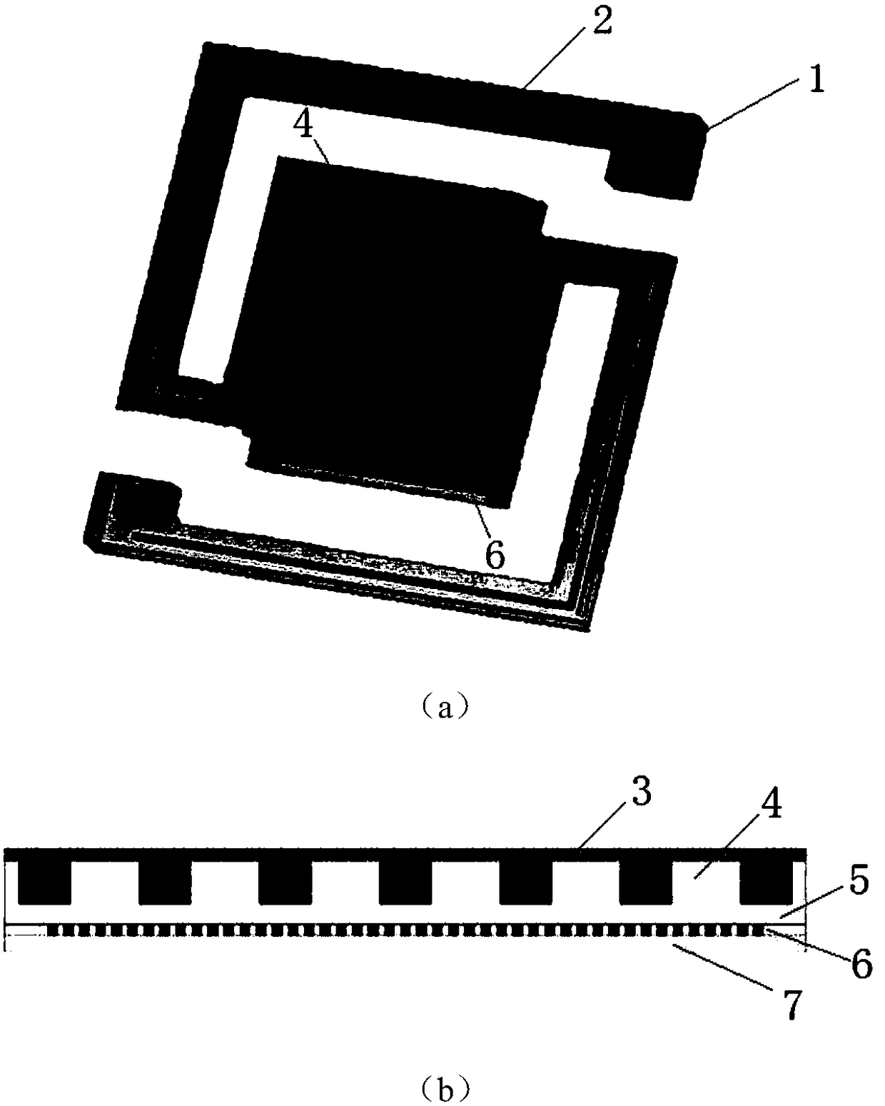
[0014] The microbolometer structure of the present embodiment is as follows figure 1 As shown, an L-shaped micro-bridge structure is adopted, and the micro-bridge structure unit includes a pier 1, a bridge arm 2 and an infrared absorber, wherein the pier 1 is used to connect the readout circuit and the supporting unit structure, and the bridge arm 2 is used to support the infrared absorber And realize the thermal isolation of the pixel; the infrared absorber mainly absorbs the infrared radiation to generate heat energy, thereby changing the resistance value of the thermistor. The infrared absorber is a multi-layer structure, from top to bottom are silicon nitride layer 3, metal grating layer 4, silicon dioxide layer 5, serpentine aluminum thermistor layer 6 and silicon...


PUM


Abstract

The invention discloses a high-performance CMOS infrared micro bolometer based on surface electromagnetic wave resonance. The micro bolometer comprises an L-shaped micro bridge structure. The micro bridge structure comprises bridge piers, bridge arms and an infrared absorbing member. The infrared absorbing member has a multilayer structure which is composed of a silicon nitride layer, a metal grating layer, a silicon dioxide layer, a zigzag aluminum heat-sensitive resistor layer and a silicon dioxide layer, wherein the silicon nitride layer, the metal grating layer, the silicon dioxide layer,the zigzag aluminum heat-sensitive resistor layer and the silicon dioxide layer are successively arranged from top to bottom. Compared with a traditional micro bolometer structure, the micro bolometerstructure is advantageous in that the metal grating is added above the heat-sensitive resistor layer, thereby forming an MIM structure. The CMOS infrared micro bolometer utilizes a surface electromagnetic wave for exciting resonance, thereby remarkably improving infrared absorbility of a detector, improving detector response and realizing high-efficiency detection. Furthermore the micro bolometeraccording to the invention is based on a standard CMOS integrated circuit process and has advantages of easy process realization, low cost, etc.

Description

technical field [0001] The invention relates to the field of infrared detection, in particular to a metal / medium / metal (MIM) structure design based on surface electromagnetic wave excitation resonance. Background technique [0002] Infrared technology is widely used in the field of security monitoring, car night vision system, medical equipment industry, home electronics industry, and communication. Uncooled infrared detectors have the advantages of light weight, low power consumption, low cost, small size and convenient operation due to the omission of complex refrigeration systems. In recent years, uncooled infrared detectors have gradually replaced cooled infrared detectors and become mainstream products for civilian use. Uncooled infrared detectors mainly include microbolometers, pyroelectric infrared detectors, thermopile infrared detectors, etc. [0003] The microbolometer is the most widely used uncooled infrared detector. Its basic principle is that the infrared abs...

Claims


Application Information

Patent Timeline
Patent Type & Authority Applications(China)
IPC IPC(8): G01J5/20
CPCG01J5/20
Inventor 纪小丽张朝阳杨琪轩沈凡翔黄延段佳华朱晨昕司伟闫锋
Owner NANJING UNIV
Why Eureka
Try Eureka