Organic transistor with transverse high-order structure

An organic transistor and transistor technology, applied in semiconductor devices, electric solid devices, semiconductor/solid device manufacturing, etc., can solve the problems of short channel length, channel width or density cannot be further increased, and organic materials cannot be used to achieve high The effects of high current density, good chemical and thermal stability, and good photoelectric properties

Inactive Publication Date: 2019-01-29
HARBIN UNIV OF SCI & TECH
View PDF4 Cites 0 Cited by
  • Summary
  • Abstract
  • Description
  • Claims
  • Application Information

AI Technical Summary

Problems solved by technology

[0002] Organic transistors can be used as driving elements in flexible displays, and organic vertical transistors such as static-sensing transistors (SITs) are suitable for high-speed switching because of their short channel length and wide channel width, however, it is difficult for organic vertical devices to Fabricate microstructures laterally, because conventional microfabrication processes, such as photolithography, plasma etching, and ion implantation, cannot be used for organic materials, and channel width or density cannot be further increased due to such limitations

Method used


Image

  • Organic transistor with transverse high-order structure
  • Organic transistor with transverse high-order structure
  • Organic transistor with transverse high-order structure

Examples


Embodiment 1

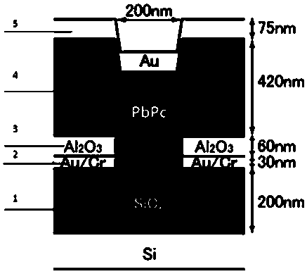
[0024] An organic transistor with a lateral high-order structure, the composition of which includes: Si / SiO 2 A substrate (1), the substrate is connected to the source Au / Cr film layer (2), and the source is connected to the insulating layer Al 2 o 3 The thin film layer (3), the active layer PbPc thin film layer (4) is connected to the substrate, and the drain Au thin film layer (5) is connected to the active layer PbPc thin film layer.

[0025] The described organic transistor with a lateral high-order structure is characterized in that: the SiO 2 The thickness is 200nm, the thickness of the source electrode Au / Cr film layer is 30nm, the insulating layer Al 2 o 3 The thickness of the active layer PbPc film is 60nm, the thickness of the active layer PbPc film is 420 nm, the thickness of the drain Au film is 75nm, the attached figure 1 is a device structure with a thickness of each layer.

Embodiment 2

[0027] A method for fabricating an organic transistor with a lateral high-order structure. The fabrication method adopts a polystyrene (PS) sphere masking method, spreading polystyrene (PS) spheres on a substrate, and after the particles are spread, sequentially spread them on the sample Deposition of Cr, Au and Al 2 o 3 , deposited Cr / Au / Al 2 o 3 After that, particles are selectively removed, PbPc is deposited by evaporation, and finally, gold electrodes are deposited.

[0028] The method for manufacturing an organic transistor with a lateral high-order structure is characterized in that: the substrate is Si / SiO 2 , the thickness of silica was 200 nm, the substrate was cleaned by ultrasonic agitation in acetone, and exposed to UV / O at 150 °C 3 For 30 min, the PS spheres were spread on the substrate using the dipping method, and the substrate was immersed in the PS sphere solution dispersed with ultrapure water for 3 h, the excess PS particles were rinsed off in ultrapu...

Embodiment 3

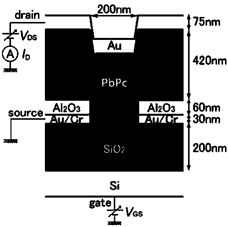
[0031] A kind of organic transistor with lateral high-order structure described in embodiment 1 or 2, Si / SiO2 substrate, Au / Cr film layer as source electrode, Si substrate as gate, Al 2 o 3The thin film layer is used as an insulating layer, the Au thin film layer is used as a drain electrode, and the PbPc / Au is used as a high-order structure to form a vertical stacked structure.

[0032] The source and drain are arranged vertically through organic semiconductors, and all transistors are connected in parallel, effectively increasing the current density.

[0033] attached figure 2 It is a characteristic test circuit diagram of an organic transistor with a lateral high-order structure.


PUM


Abstract

The invention discloses an organic transistor with a transverse high-order structure. At present, a new concept ''high-order structure spontaneous patterning'' (SPHOS) manufacturing technology has been used for studying vertical devices. The invention adopts a polystyrene (PS) sphere masking method to prepare the organic transistor with the transverse high-order structure. The organic transistor comprises a Si / SiO2 substrate (1), wherein the upper surface of the substrate is connected with a source Au / Cr thin film layer (2), the upper surface of the source is connected with an insulating layer Al2O3 thin film layer (3), the upper surface of the substrate is connected with an active layer PbPc thin film layer (4), and the upper surface of active layer PbPc thin film layer (4) is connectedwith a drain Au thin film layer (5). The organic transistor is used in the fields of liquid crystal panel driving, organic integrated circuit chips, and other electronic circuits.

Description

technical field [0001] The invention relates to an organic transistor with a lateral high-order structure. Background technique [0002] Organic transistors can be used as driving elements in flexible displays, and organic vertical transistors such as static-sensing transistors (SITs) are suitable for high-speed switching because of their short channel length and wide channel width, however, it is difficult for organic vertical devices to Microstructures are fabricated laterally because conventional microfabrication processes, such as photolithography, plasma etching, and ion implantation, cannot be used for organic materials, and the channel width or density cannot be further increased due to such limitations. [0003] In recent years, vertical-type devices have been studied using fabrication techniques based on a new concept of "spontaneous patterning of higher-order structures." Using these techniques, we can fabricate lateral higher-order structures in large-scale organi...

Claims


Application Information

Patent Timeline
Patent Type & Authority Applications(China)
IPC IPC(8): H01L51/05H01L51/40
CPCH10K10/491
Inventor 王东兴张志文
Owner HARBIN UNIV OF SCI & TECH
Why Eureka
Try Eureka