
Method for low-pressure sintering hybrid power module by nano-silver solder paste

A mixed-power, low-pressure sintering technology, which is applied to semiconductor/solid-state device components, semiconductor devices, electrical components, etc., can solve problems such as unsuitable pressure, large area difference, and easy damage of SiC diode chips.

Inactive Publication Date: 2019-02-22
TIANJIN UNIV
View PDF6 Cites 1 Cited by
  • Summary
  • Abstract
  • Description
  • Claims
  • Application Information

AI Technical Summary

Problems solved by technology

[0004] However, when the hybrid power module is sintered and packaged with nano silver solder paste, the SiIGBT chip area inside the hybrid power module is relatively large (≥100mm2), and the SiC diode chip area is relatively small (≤25mm2). The chip is easy to damage and should not be pressurized. The existing technology cannot achieve the simultaneous sintering of two chips on the bare copper substrate, and the solder paste layer obtained has high strength. This requires a method to solve this problem and realize nano silver soldering Capabilities of Paste-Encapsulated Hybrid Power Modules

Method used


Image

  • Method for low-pressure sintering hybrid power module by nano-silver solder paste
  • Method for low-pressure sintering hybrid power module by nano-silver solder paste
  • Method for low-pressure sintering hybrid power module by nano-silver solder paste

Examples


Embodiment 1

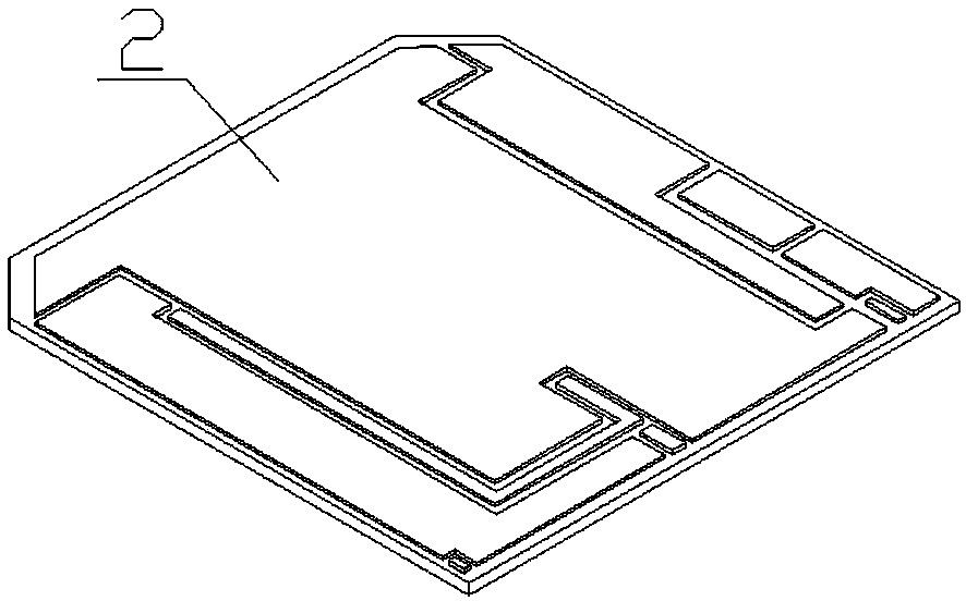
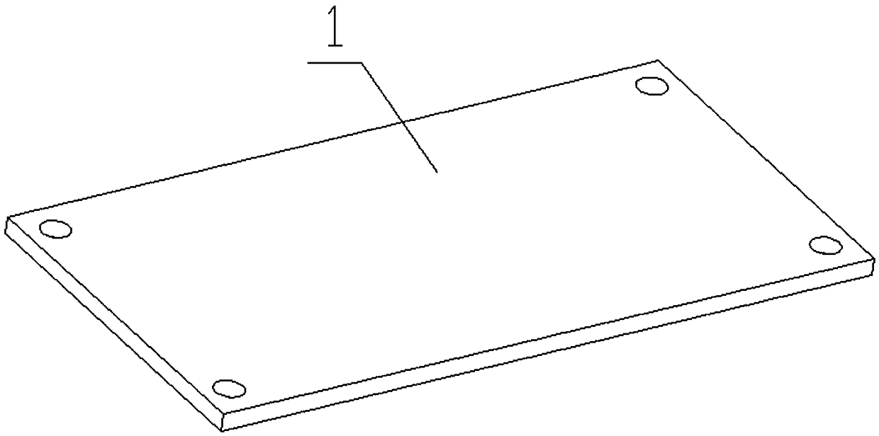
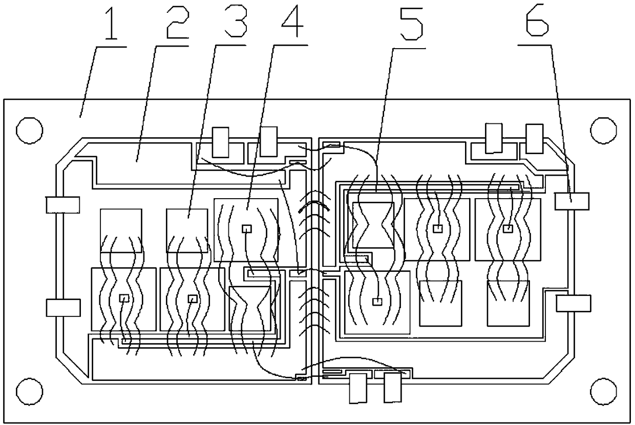
[0035] Example 1: Ultrasonic cleaning of copper-clad substrate (2) and copper base plate (1), then printing nano-silver solder paste on the substrate (2) and patch wetting; pre-drying: first put the sample on the heating table to heat Pre-drying at 90°C and holding for 10 minutes; pressurization: apply a pressure of 2 MPa to the large-area Si-based IGBT chip (4), and no pressure on the small-area SiC diode chip (3); sintering: then increase the temperature at a rate of 5°C / min Heating at a rate of 270°C and keeping it warm for 20 minutes in a mixed atmosphere of 50% air + 50% nitrogen; reduction: followed by vacuuming and nitrogen formic acid mixture for 10 minutes. After sintering and molding, the shear strengths of the chips in both areas reach above 30MPa. After sintering, follow-up processes such as wire bonding, secondary welding, housing installation, glue coating and sealing, and sealing agent filling are carried out.

Embodiment 2

[0036] Embodiment 2: Ultrasonic cleaning of the copper-clad substrate (2) and the copper base plate (1), and then printing nano-silver solder paste on the substrate (2) and patch wetting. Pre-drying: first heat the sample on a heating table to 100°C and keep it warm for 12 minutes to complete the pre-drying; pressurization: apply a pressure of 2 MPa to the large-area Si-based IGBT chip (4), and apply a pressure of 2 MPa to the small-area SiC diode chip (3) Pressurized; sintering: then heated to 270°C at a heating rate of 5°C / min and kept in a 50% air + 50% nitrogen mixed atmosphere for 20 minutes; reduction: followed by vacuuming and nitrogen formic acid mixture for 10 minutes. After sintering and molding, the shear strengths of the chips in both areas reach above 30MPa. After sintering, follow-up processes such as wire bonding, secondary welding, housing installation, glue coating and sealing, and sealing agent filling are carried out.

Embodiment 3

[0037]Embodiment 3: Ultrasonic cleaning of the copper-clad substrate (2) and the copper base plate (1), and then printing nano-silver solder paste on the substrate (2) and patch wetting. Pre-drying: first heat the sample on a heating table to 90°C and keep it warm for 10 minutes to complete the pre-drying; pressurization: apply a pressure of 2 MPa to the large-area Si-based IGBT chip (4), and apply a pressure of 2 MPa to the small-area SiC diode chip (3). Pressurization; sintering: then heated to 280°C at a heating rate of 5°C / min and kept in a 50% air + 50% nitrogen mixed atmosphere for 30 minutes; reduction: followed by vacuuming and nitrogen formic acid mixture for 12.5 minutes. After sintering and molding, the shear strengths of the chips in both areas reach above 30MPa. After sintering, follow-up processes such as wire bonding, secondary welding, housing installation, glue coating and sealing, and sealing agent filling are carried out.


PUM

PropertyMeasurementUnit
areaaaaaaaaaaa
shear strengthaaaaaaaaaa

Abstract

The invention provides a method for low-pressure sintering a hybrid power module by nano-silver solder paste. The method can simultaneously sinter two chips with a large area difference and can obtaina solder paste layer having a high strength (>=30 MPa). The method comprises four processes including pre-drying, pressurizing, sintering, and reducing. The pre-drying process is to provide a certainviscosity for the solder paste to avoid the overflow of the excessive solder paste during the pressurizing process of a large-area chip. The pressurization process is to pressurize the large-area Sichip to promote the sintering, and not to pressurize the small-area SiC chip to avoid damage. The sintering process is carried out under a 50% air + 50% nitrogen atmosphere to ensure sufficient oxygen for the sintering of the solder paste and to avoid the oxide formation on the substrate surface. The reducing process is to reduce the surface oxide of the substrate by formic acid to remove copperoxide formed on the surface. The overall process flow of the invention is relatively simple, and is suitable for the manufacture of a hybrid power module having a large chip area difference.

Description

technical field [0001] The invention relates to the field of packaging of power electronic devices, in particular to a method for low-pressure sintering of nano-silver solder paste and a hybrid power module. Background technique [0002] Silicon carbide (SiC) material has the advantages of high thermal conductivity, high breakdown electric field strength and large forbidden band width, which makes SiC devices exhibit better high temperature characteristics, lower power consumption and faster switching speed. In recent years, with the further development of SiC material technology, SiC high-power modules in the field of power electronic devices have gradually become a research and development hotspot. Studies have shown that using SiC Schottky diodes to replace traditional Si diodes, and a hybrid power module composed of Si-based IGBTs can reduce the on-state loss and switching loss of the power module. [0003] Traditional hybrid power modules use solder alloys with low mel...

Claims


Application Information

Patent Timeline
Patent Type & Authority Applications(China)
IPC IPC(8): H01L25/07H01L23/488H01L21/60
CPCH01L24/03H01L25/071H01L23/488H01L2924/19107H01L2224/0603H01L2224/48139H01L2224/49111H01L2224/49113
Inventor 梅云辉邓文斌李欣陆国权
Owner TIANJIN UNIV
Learn More