Check patentability & draft patents in minutes with Patsnap Eureka AI!

Silicon-based microdisplay pixel circuit with high uniformity and low leakage

A technology of display pixel and uniformity, applied in the field of silicon-based microdisplay pixel circuit, can solve problems such as affecting the display quality of OLED, and achieve the effects of stabilizing the voltage of the gate, reducing leakage and improving non-uniformity

Inactive Publication Date: 2019-03-01
NO 55 INST CHINA ELECTRONIC SCI & TECHNOLOGYGROUP CO LTD
View PDF9 Cites 6 Cited by
  • Summary
  • Abstract
  • Description
  • Claims
  • Application Information

AI Technical Summary

Problems solved by technology

At the same time, due to the continuous leakage of the MOS switch in the pixel unit when it is turned off, it will also affect the OLED display quality

Method used


Image

  • Silicon-based microdisplay pixel circuit with high uniformity and low leakage
  • Silicon-based microdisplay pixel circuit with high uniformity and low leakage

Examples


Embodiment Construction

[0018] The present invention will be described in detail below in conjunction with the accompanying drawings and specific embodiments.

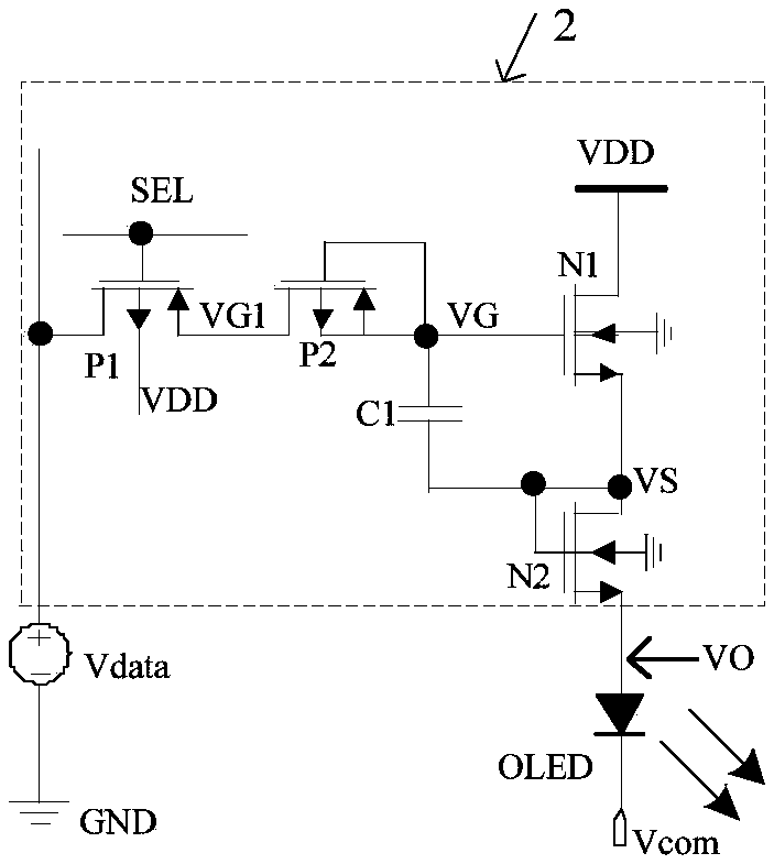
[0019] Such as figure 2 shown.

[0020] A silicon-based micro-display pixel circuit with high uniformity and low leakage, which is composed of a specific pixel circuit 2 in a dotted line frame, an external voltage source Vdata, and an external OLED, specifically including a driving tube N1, a switching tube P1, a switching tube P2, and a switching tube N2 , storage capacitor C1; the drain of the P-type MOS transistor P1 is connected to the positive end of the input voltage source Vdata, the source of the P-type MOS transistor P1 is connected to the drain of the P-type MOS transistor P2, and the substrate of the P-type MOS transistor P1 It is connected to the power supply VDD, and the gate of the P-type MOS transistor P1 is connected to the row selection control signal SEL2. The negative end of the voltage source Vdata is connected to the g...


PUM


Abstract

Provided is a silicon-based microdisplay pixel circuit with high uniformity and low leakage. The invention provides a novel pixel circuit, comprising a driving tube N1, a switching tube P1, a switching tube P2, a switching tube N2 and a storage capacitor C1. The invention provides an improved 4T1C pixel circuit based on an existing 2T1C pixel circuit. The circuit is added with a transistor N2 connected in the form of a diode and a transistor P2 connected in the form of a diode on the basis of an existing pixel circuit. Under different process deviations, when threshold voltage of the driving tube N1 changes, resistance of the transistor N2 follows the change, and finally the amount of change of VO due to threshold voltage shift is weakened. The uniformity of OLED illumination is increased.When a row selection control signal SEL is at high level, VG point voltage continuously leaks through the P1, and the added transistor P2 has a parasitic reverse diode between a VG and a VG1, so thatleakage of the VG point is decreased, and VG voltage is more stable relative to grid voltage of a driving tube in a conventional pixel structure in Fig.1.

Description

technical field [0001] The invention relates to a microelectronics and display technology, in particular to an OLED display driving technology, in particular to a silicon-based micro-display pixel circuit with high uniformity and low leakage. Background technique [0002] Silicon-based active organic light-emitting diode (AMOLED) microdisplay is a branch of display technology, which realizes the combination of OLED technology and silicon-based integrated circuit technology. OLED micro-display technology utilizes mature CMOS integrated circuit technology. After the driver chip is manufactured, the OLED device is manufactured, thereby improving the yield rate of the entire display. OLED microdisplay has the advantages of active light emission, wide viewing angle, high luminous efficiency, fast response speed, and low power consumption. Because of its small size, it has great advantages in portable display applications. The current main applications include helmet-mounted dis...

Claims


Application Information

Patent Timeline
IPC IPC(8): G09G3/3225
CPCG09G3/3225G09G2320/0233
Inventor 秦昌兵张白雪陈啟宏杨建兵陈建军
Owner NO 55 INST CHINA ELECTRONIC SCI & TECHNOLOGYGROUP CO LTD
Features
  • R&D
  • Intellectual Property
  • Life Sciences
  • Materials
  • Tech Scout
  • Unparalleled Data Quality
  • Higher Quality Content
  • 60% Fewer Hallucinations
Learn More