Semiconductor structure and forming method thereof
A semiconductor and connecting part technology, applied in the field of semiconductor structure and its formation, can solve problems such as large contact resistance, and achieve the effects of reducing loss, improving efficiency, and improving controllability
- Summary
- Abstract
- Description
- Claims
- Application Information
AI Technical Summary
Problems solved by technology
Method used
Image


Examples
Embodiment Construction
[0030] As mentioned in the background, the contact resistance of the semiconductor device is relatively high.
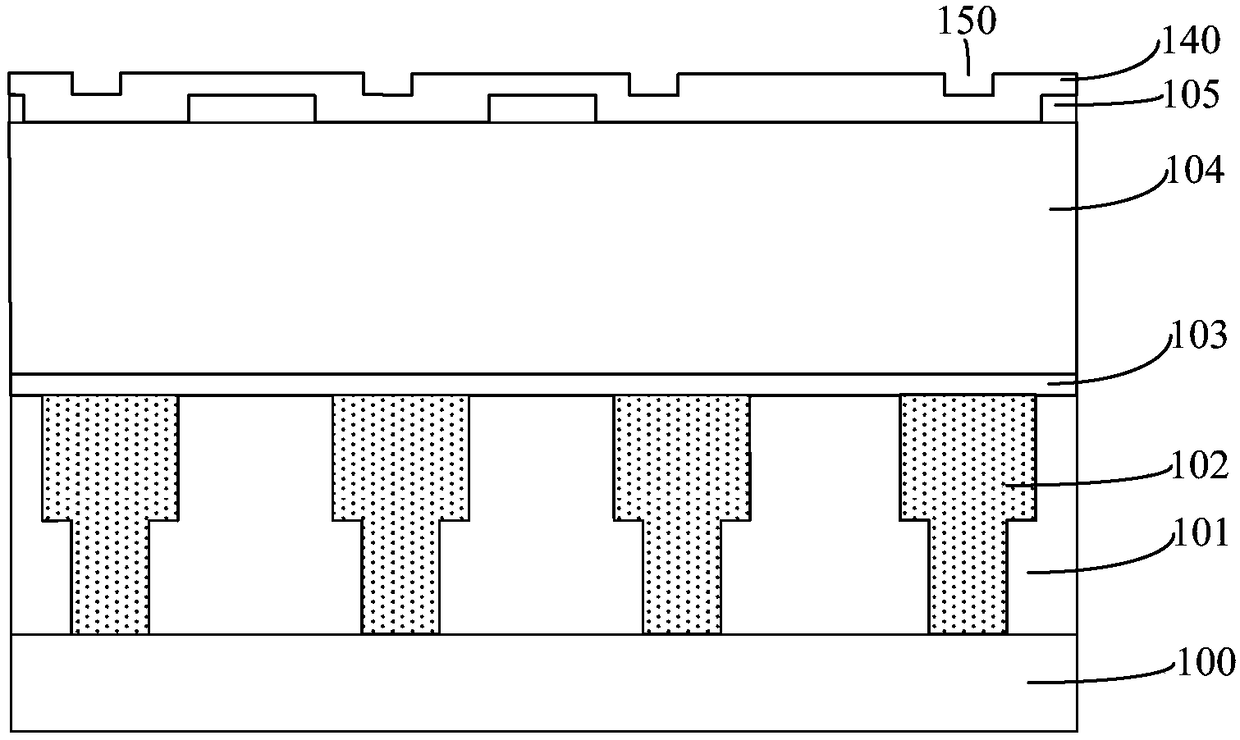
[0031] Figure 1 to Figure 3 It is a structural schematic diagram of each step of a method for forming a semiconductor structure.
[0032] Please refer to figure 1 , providing a substrate 100, the substrate 100 has a first dielectric layer 101; a first opening (not shown in the figure) is formed in the first dielectric layer 101; a first interconnection is formed in the first opening structure 102; a stop layer 103 is formed on the first dielectric layer 101 and the first interconnection structure 102; a second dielectric layer 104 is formed on the stop layer 103, and a first mask is formed on the second dielectric layer 104 The film layer 105 has a first mask opening (not shown in the figure) in the first mask layer 105; a second mask layer is arranged in the first mask opening and on the first mask layer 105 140, the second mask layer 140 has a second mask openi...
PUM
| Property | Measurement | Unit |
|---|---|---|
| Thickness | aaaaa | aaaaa |
Abstract
Description
Claims
Application Information
 - R&D
- Intellectual Property
- Life Sciences
- Materials
- Tech Scout
- Unparalleled Data Quality
- Higher Quality Content
- 60% Fewer Hallucinations
Browse by: Latest US Patents, China's latest patents, Technical Efficacy Thesaurus, Application Domain, Technology Topic, Popular Technical Reports.
© 2025 PatSnap. All rights reserved.Legal|Privacy policy|Modern Slavery Act Transparency Statement|Sitemap|About US| Contact US: help@patsnap.com