Method for improving absorption and utilization efficiency of solar energy

A solar energy and efficiency technology, applied in the field of solar energy utilization, can solve the problems of low average absorption rate, large fluctuation of absorption spectrum, low absorption of solar spectrum, etc., and achieve the effect of improving absorption and utilization efficiency.

Active Publication Date: 2019-03-08
QINGDAO UNIV
View PDF7 Cites 7 Cited by
  • Summary
  • Abstract
  • Description
  • Claims
  • Application Information

AI Technical Summary

Problems solved by technology

The article "Enhanced absorption of graphene with one-dimensional photonic crystal" mentioned that graphene can absorb uniformly in a large wavelength range, but the absorption rate is very small. After introducing a one-dimensional photonic crystal under the graphene layer, The absorption peak is at 550nm, increasing the number of graphene layers, the absorption rate will increase significantly, changing the incident angle, the greater the incident angle of the TE film, the absorption peak shifts to the left, and the absorption rate increases, but overall the total absorption rate is still very high. Small, the value of the absorption rate is about 0.3; "Research on the absorption characteristics of photonic crystal defect layer" said that the dielectric layer A is ZnSe, the dielectric layer B is Na3AlF6, the defect layer is metal Al, and there are two dielectric periods of A and B A layer of metal defects is added in the middle of the one-dimensional photonic crystal structure with a permanent arrangement. The absorption characteristics of the photonic crystal defect layer of this structure are studied, and it is concluded that the photonic crystal with metal defects in the wavelength range of 600nm-1500nm has obvious absorption of incident light. , but the average absorption rate is low, the one-dimensional photonic crystal contains only one metal layer, the absorption of the solar spectrum is low, and the absorption spectrum fluctuates greatly

Method used


Image

  • Method for improving absorption and utilization efficiency of solar energy
  • Method for improving absorption and utilization efficiency of solar energy
  • Method for improving absorption and utilization efficiency of solar energy

Examples


Embodiment Construction

[0018] The present invention will be described in detail below in combination with specific embodiments.

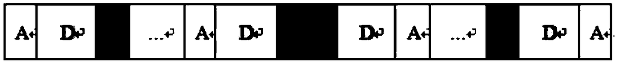
[0019] 1 One-dimensional photonic crystal bandgap structure

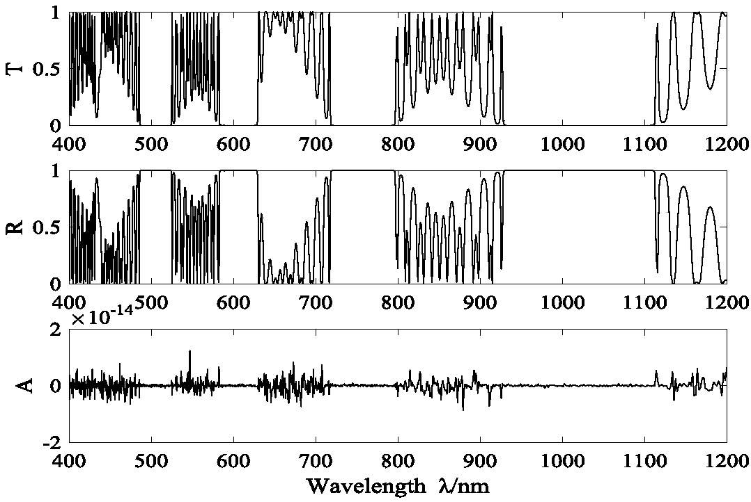
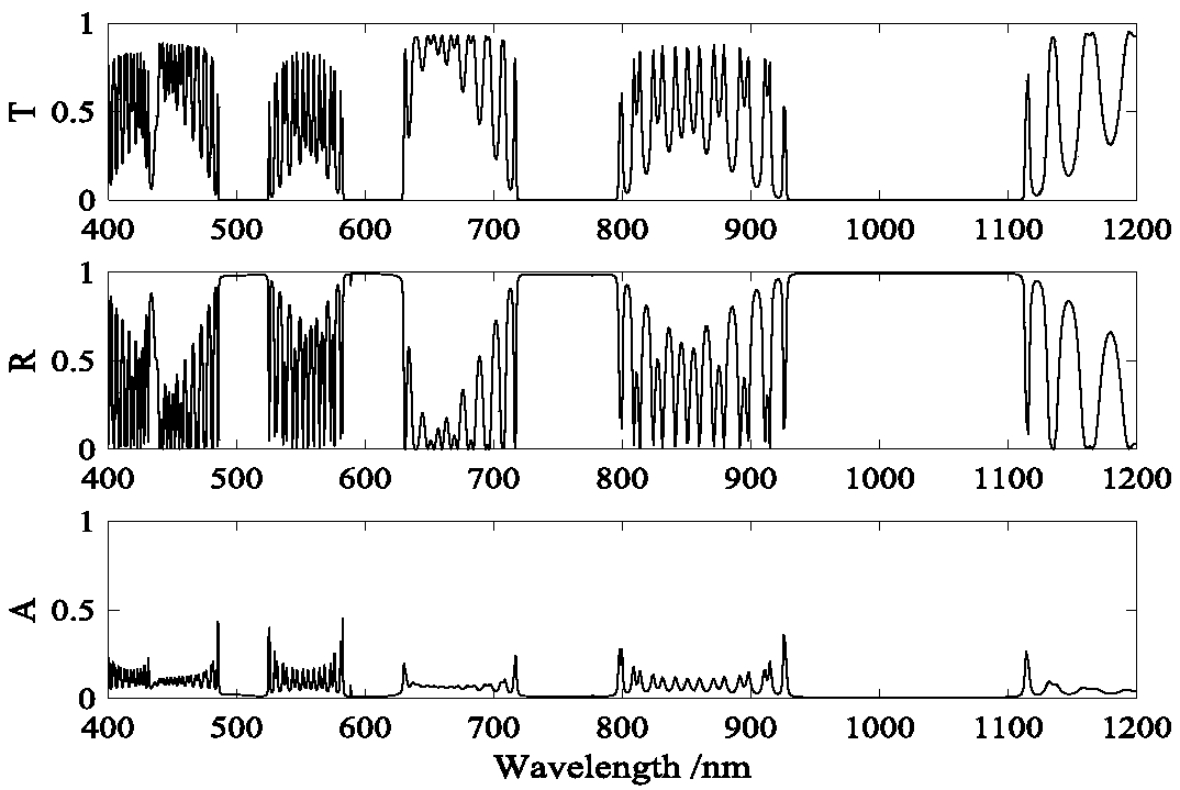
[0020] The one-dimensional photonic crystal of the present invention is made up of three kinds of materials A, B and D arranged alternately, is (ADB) 10 (BDA) 10 The periodic symmetric structure of , such as figure 1 shown. Its basic parameters, the refractive index of the dielectric material A n a =1.38, geometric thickness a=175nm, dielectric material B, refractive index n b =3.8, geometric thickness b=175nm, material D is metal material, refractive index n d =1.74+0.001i, geometric thickness d=350nm. The center wavelength is taken as λ 0 =700nm, the research wavelength ranges from visible light to near-infrared 400-1200nm solar spectrum, and the incident light is TE wave of vertical incidence.

[0021] Using the method of transmission matrix to study the absorption characteristics, the propagation of...


PUM

PropertyMeasurementUnit
thicknessaaaaaaaaaa
thicknessaaaaaaaaaa
wavelengthaaaaaaaaaa

Abstract

The invention discloses a method for improving the absorption and utilization efficiency of solar energy. A one-dimensional photonic crystal is formed by materials A, materials B and materials C whichare alternately arranged and is of a periodical symmetrical structure of (ADB)10*BDA)10. The refractivity na of the dielectric materials A is 1.38, and the geometric thickness a of the dielectric materials A is 175 nm. The refractivity nb of the dielectric materials B is 3.8, and the geometric thickness b of the dielectric materials B is 175 nm. The refractivity nd of the dielectric materials D meets the equation nd+1.74+0.01i, and the geometric thickness d of the dielectric materials A is 350 nm. The influences of the extinction coefficient, the dispersion coefficient and the periodicity ofthe photonic crystal structure of the absorptivity are studied, so that the method has the beneficial effects that absorption of solar energy can be effectively improved, and the utilization efficiency of the solar energy is improved accordingly.

Description

technical field [0001] The invention belongs to the technical field of optical materials, and relates to the absorption of solar radiation, the design of photonic crystals and the utilization of solar energy. Background technique [0002] Photonic crystals are artificially designed and fabricated microstructure materials with periodic dielectric structures on the optical scale. Due to the introduction of certain defects in the photonic crystal periodic structure, there will be a defect state with a very narrow frequency in its forbidden band, and the photons with the same frequency as the defect state may be localized at the defect position. Once it deviates from the defect position, the light will Decays rapidly. Based on this, photonic crystals can be applied to many aspects, such as lossless photonic crystal waveguides, high-performance filters, photonic crystal polarizers, and photonic crystal fibers. [0003] Introducing absorbing materials into the photonic crystal s...

Claims


Application Information

Patent Timeline
Patent Type & Authority Applications(China)
IPC IPC(8): F24S70/12G02B1/00
CPCG02B1/005
Inventor 李长红单圆圆张楠方雨帆
Owner QINGDAO UNIV
Why Eureka
Try Eureka