Deep ultraviolet light emitting diode chip and preparation method thereof

A light-emitting diode and deep ultraviolet technology, applied in semiconductor devices, electrical components, circuits, etc., can solve problems such as chip light efficiency decline, accelerated device degradation, uneven heat distribution, etc., to improve wall plug efficiency, reduce Joule heat, The effect of small series resistance

Active Publication Date: 2020-07-31
EZHOU INST OF IND TECH HUAZHONG UNIV OF SCI & TECH +1
View PDF12 Cites 0 Cited by
  • Summary
  • Abstract
  • Description
  • Claims
  • Application Information

AI Technical Summary

Problems solved by technology

As far as the light efficiency of deep ultraviolet LED is concerned, uneven current density distribution will inevitably lead to uneven carrier radiative recombination in the active area, so the proportion of light energy emitted from the active area escaping to the outside of the chip will also occur. Changes, so the uneven current density distribution will lead to a decrease in the light efficiency of the chip
On the other hand, a large amount of Joule heat will be generated in places where the current is dense, especially in the active area near the n-type electrode. Due to the injection of a large number of carriers, the proportion of non-radiative recombination and Auger recombination in the active area will decrease. Relatively increased, then the active region will be affected by the uneven heat distribution and the decrease of the internal and external quantum efficiency caused by the temperature
At the same time, due to the high junction temperature of the device, local overheating will cause electromigration of metals, material aging, etc., which will accelerate device degradation and lead to chip failure.

Method used


Image

  • Deep ultraviolet light emitting diode chip and preparation method thereof
  • Deep ultraviolet light emitting diode chip and preparation method thereof
  • Deep ultraviolet light emitting diode chip and preparation method thereof

Examples


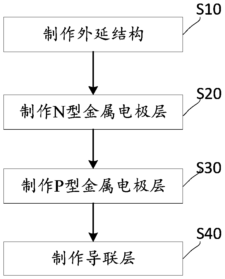
Embodiment Construction

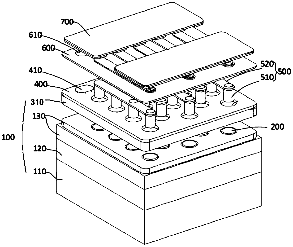
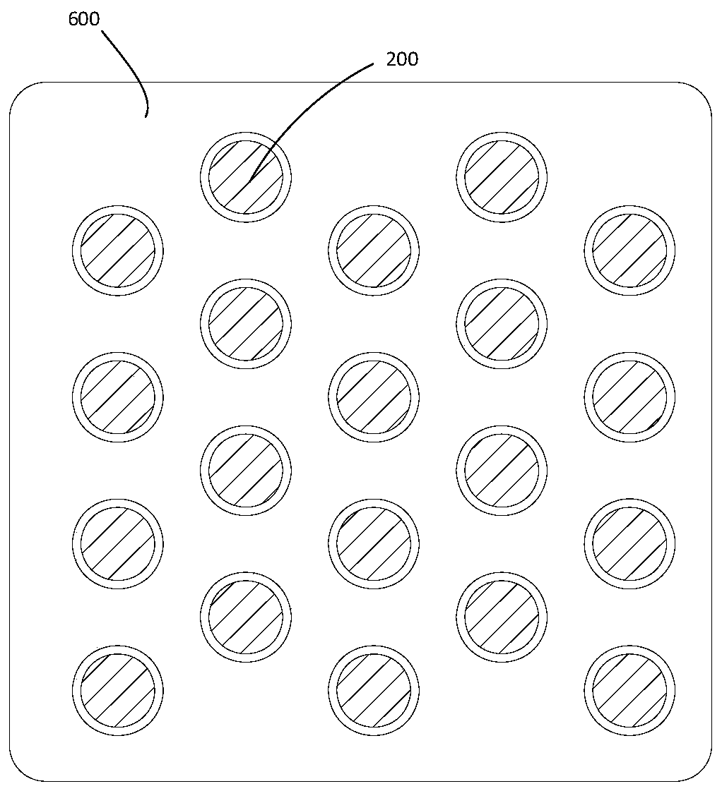
[0029] In order to facilitate the understanding of the present invention, the present invention will be described more fully below with reference to the associated drawings. Preferred embodiments of the invention are shown in the accompanying drawings. However, the present invention can be embodied in many different forms and is not limited to the embodiments described herein. On the contrary, these embodiments are provided to make the understanding of the disclosure of the present invention more thorough and comprehensive.

[0030] It should be noted that when an element is referred to as being “fixed” to another element, it can be directly on the other element or there can also be an intervening element. When an element is referred to as being "connected to" another element, it can be directly connected to the other element or intervening elements may also be present.

[0031] Unless otherwise defined, all technical and scientific terms used herein have the same meaning as...


PUM

PropertyMeasurementUnit
diameteraaaaaaaaaa
thicknessaaaaaaaaaa
thicknessaaaaaaaaaa

Abstract

The invention relates to a novel deep-ultraviolet light-emitting diode chip comprising an epitaxial structure and a P type metal electrode layer arranged on the epitaxial structure. A plurality of holes are formed in the P type metal electrode layer; and the positions of the adjacent two layers of holes correspond to each other. In addition, the chip also includes an N type metal electrode layer and a connecting layer. The N type metal electrode layer includes a plurality of columns of electrode posts; each column of electrode posts includes a plurality of sub electrode posts that are connected in the holes of an N-AlGaN layer one by one, wherein the diameters of the electrode pots are smaller than the diameters of the holes; and the central space between every two adjacent sub electrode posts is equal. In addition, the invention also relates to a preparation method of a novel deep-ultraviolet light-emitting diode chip. Compared with the conventional long-bar-shaped electrode deep-ultraviolet LED, the provided deep-ultraviolet light-emitting diode has the substantially improved wall plugging efficiency; the heat losses caused by work are reduced substantially; and thus the servicelife of the product is further prolonged.

Description

technical field [0001] The invention relates to the field of design and preparation of semiconductor devices, in particular to a deep ultraviolet light-emitting diode chip and a preparation method thereof. Background technique [0002] AlGaN-based deep ultraviolet light-emitting diodes have received continuous attention due to their wide range of applications, such as air purification, sterilization, biochemical detection, and optical communications. Wafers epitaxially grown on c-plane sapphire substrates by metal-organic compound chemical vapor deposition (MOCVD), due to the insulation of the substrate sapphire, in the process of device preparation, the wafer must be etched by etching The surface of the chip forms a mesa structure, that is, the n-type electrode and the p-type electrode are on the same side. In this mesa structure, there is inevitably a problem of lateral current spreading, which leads to current concentration at the edge of the mesa. Moreover, with the in...

Claims


Application Information

Patent Timeline
Patent Type & Authority Patents(China)
IPC IPC(8): H01L33/38
CPCH01L33/382H01L33/387H01L2933/0016
Inventor 张爽张会雪王帅戴江南陈长清
Owner EZHOU INST OF IND TECH HUAZHONG UNIV OF SCI & TECH
Why Eureka
Try Eureka