Surface plasmon lens design method used for nano-gap type near-field lithography

A surface plasmon and nano-gap technology, applied in the field of nano-processing, can solve the problems of poor graphics quality, low depth and width of nano-pattern processing, etc., and achieve high resolution, enhanced etching ability, and low-cost effects

Active Publication Date: 2019-03-29
CHINA UNIV OF PETROLEUM (EAST CHINA)
View PDF5 Cites 0 Cited by
  • Summary
  • Abstract
  • Description
  • Claims
  • Application Information

AI Technical Summary

Problems solved by technology

[0006] The purpose of the present invention is to provide a surface plasmon lens design method for nano-gap near-field lithography to solve the problems of low aspect ratio and poor image quality in nano-pattern processing of rotating field

Method used


Image

  • Surface plasmon lens design method used for nano-gap type near-field lithography
  • Surface plasmon lens design method used for nano-gap type near-field lithography
  • Surface plasmon lens design method used for nano-gap type near-field lithography

Examples


Embodiment Construction

[0044] The following describes the embodiments of the present invention in detail, and those skilled in the art will understand that the following embodiments are intended to explain the present invention, and should not be regarded as limiting the present invention. Unless otherwise specified, if the specific techniques or conditions are not clearly described in the following examples, those skilled in the art can carry out according to the commonly used techniques or conditions in this field or according to the product instructions. The reagents or instruments used were not indicated by the manufacturer, and they were all conventional products available in the market.

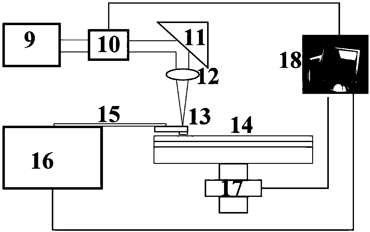
[0045] A method for designing a surface plasmon lens for nano-gap near-field lithography according to the present invention, specifically comprising the following steps:

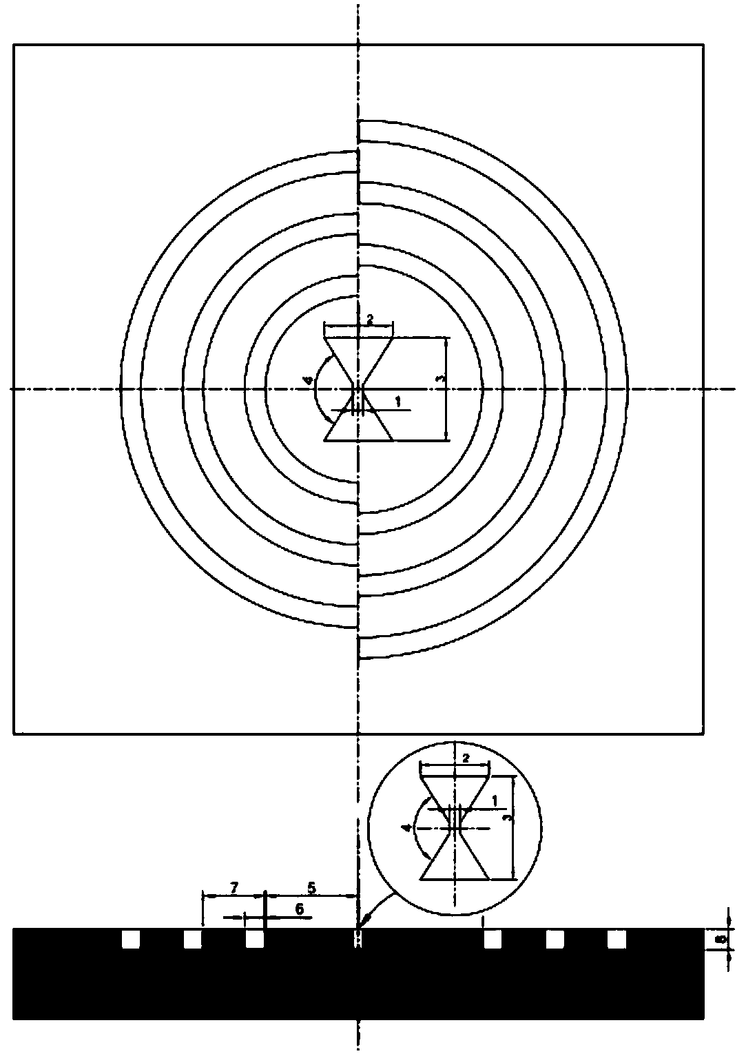
[0046] (1) First prepare a surface plasmon lens with an alternating composite structure of bowknot and concentric semicircular grooves. Th...


PUM

PropertyMeasurementUnit
thicknessaaaaaaaaaa
thicknessaaaaaaaaaa
thicknessaaaaaaaaaa

Abstract

The invention discloses a surface plasmon lens design method used for nano-gap type near-field lithography. According to the propagation characteristic of surface plasmons on the surface of an air/ photoresist multilayer continuous dielectric, a concentric alternating semi-circular groove structure which enables beams to achieve super-diffraction-limited bunching in a nano-gap layer and maintain the bunching ability in a photoresist layer is designed. An ultra-small bow structure is designed at the center of the semi-circular groove is designed to excite a local surface plasmon with super-binding ability. The etching ability of a bunching light spot to penetrate the photoresist layer in the longitudinal direction is further enhanced. The concentric alternating semi-circular groove bow composite structure can form reflection electromagnetic wave coupling with a nanostructured metal film layer prepared on the surface of a disk. The energy-enhanced and small-sized bunching light spot is formed at the center of the bow, which helps to improve the depth-to-width ratio of nano-pattern processing. High-efficiency, high-resolution and low-cost nanofabrication can be realized.

Description

technical field [0001] The invention belongs to the technical field of nano-processing, and relates to a surface plasmon excitation method for realizing large aspect ratio near-field optical etching, in particular to a surface plasmon lens for nano-gap near-field lithography design method. Background technique [0002] Optical exposure is the use of optical imaging to image the mask pattern onto the photoresist surface. During the processing, the resolution of the processed pattern is an important basis for measuring the integration of the processed pattern. Limited by the optical diffraction limit, to obtain smaller processing size and higher processing resolution, higher resolution can be obtained by reducing the wavelength of incident light, increasing optical numerical aperture or reducing process parameters. Some methods that can break through the diffraction limit can also be used to achieve super-resolution beamforming. For the photolithography technology commonly u...

Claims


Application Information

Patent Timeline
Patent Type & Authority Applications(China)
IPC IPC(8): G02B5/00G03F7/20
CPCG02B5/008G03F7/20
Inventor 纪佳馨徐鹏飞吴宝贵李静
Owner CHINA UNIV OF PETROLEUM (EAST CHINA)
Why Eureka
Try Eureka