Method for preparing low-voltage driving organic light-emitting diode in p-i-n structure by solution method

A p-i-n, light-emitting diode technology, applied in semiconductor/solid-state device manufacturing, electrical components, circuits, etc., can solve the problems of low carrier mobility, lower device drive voltage, high device drive voltage, etc., to improve transmission performance, The effect of lowering the driving voltage and lowering the hole injection barrier

Active Publication Date: 2019-04-05
BINHAI IND RES INST OF TIANJIN UNIV CO LTD
View PDF6 Cites 2 Cited by
  • Summary
  • Abstract
  • Description
  • Claims
  • Application Information

AI Technical Summary

Problems solved by technology

[0004] The purpose of the present invention is to solve the problems in the prior art that the carrier mobility in the transport layer prepared by the solution method is not high, the film-forming property is not good, the driving voltage of the device is high, and the luminescence performance is poor, and a solution method is provided. The p-i-n structure organic light-emitting diode (OLED) method, by introducing the composite material PTAA:AgNWs into the OLED device, can effectively improve the transport performance of the hole transport layer and reduce the hole injection barrier, thereby reducing the drive of the device. Voltage; PEI:SnS prepared by solution method 2 -QDs serve as the electron transport layer of OLED devices, further improving the electron injection and transport capabilities in the device

Method used


Image

  • Method for preparing low-voltage driving organic light-emitting diode in p-i-n structure by solution method
  • Method for preparing low-voltage driving organic light-emitting diode in p-i-n structure by solution method
  • Method for preparing low-voltage driving organic light-emitting diode in p-i-n structure by solution method

Examples


Embodiment 1

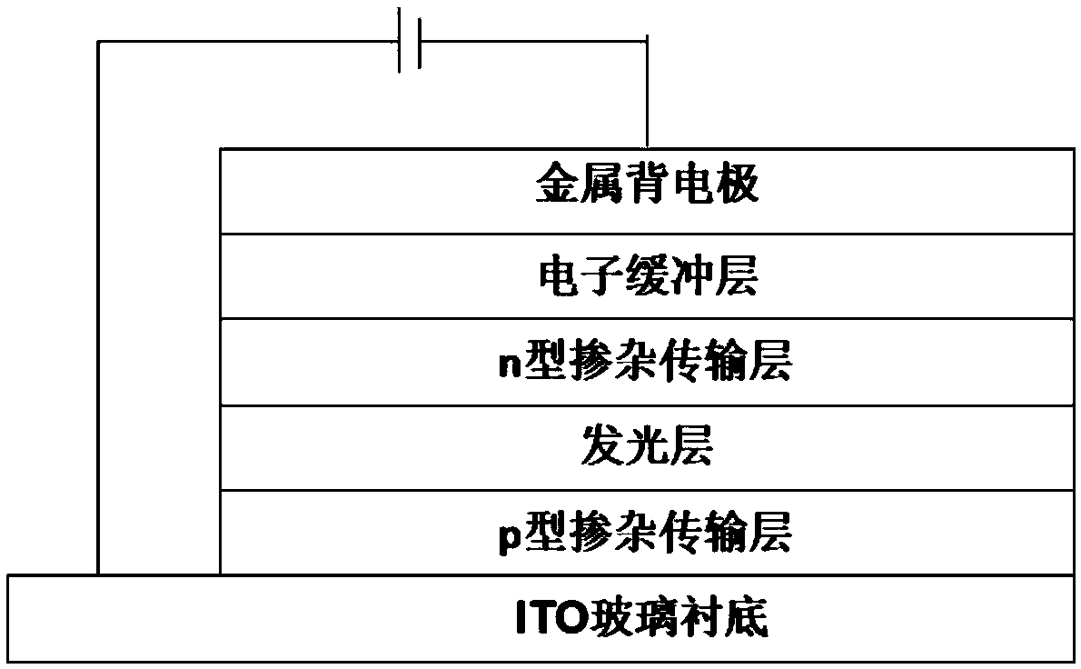
[0032] A solution method for preparing a p-i-n structure low-voltage driving organic light-emitting diode, the specific implementation steps are as follows:

[0033] 1. Etching of ITO glass substrate: The ITO glass substrate is chemically etched to form a strip electrode, and the etched ITO glass substrate is ultrasonically cleaned with ethanol, acetone, and isopropanol for 15 minutes, and then cleaned with deionized water. Rinse and dry at 150°C for 30 minutes;

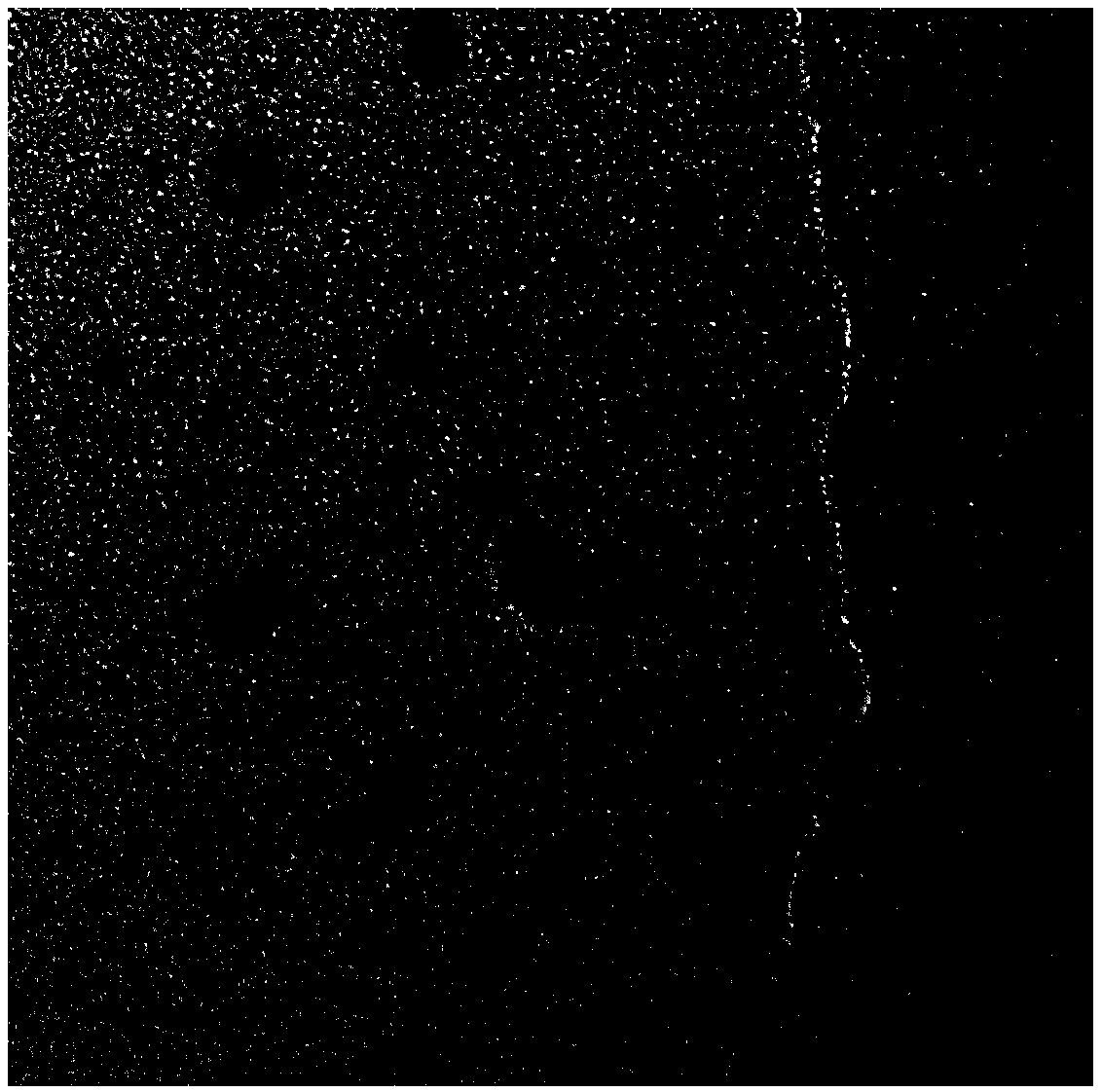
[0034]2. Preparation of the p-type doped transport layer: Weigh 10 mg of PTAA powder with an electronic balance and dissolve it in toluene solution to prepare a PTAA solution with a concentration of 10 mg / ml. AgNWs were dispersed in ethanol solution at a concentration of 10 mg / ml (eg figure 2 shown). The PTAA solution and the AgNWs solution were uniformly mixed at a volume ratio of 20:1 to prepare a PTAA:AgNWs mixed solution. Place the spare ITO glass substrate in step 1 on the homogenizer, take an appropriate am...

Embodiment 2

[0040] The specific implementation method is different except following conditions, and other is identical with embodiment 1:

[0041] Preparation of the p-type doped transport layer: 10 mg of PTAA powder was weighed with an electronic balance and dissolved in toluene solution to prepare a PTAA solution with a concentration of 10 mg / ml. Mix the PTAA solution with the AgNWs solution at a concentration of 10 mg / ml at a volume ratio of 30:1. Place the spare ITO glass substrate in step 1 on the homogenizer, take an appropriate amount of PTAA:AgNWs mixed solution and drop it on the ITO glass substrate, spin-coat at a speed of 1500rpm for 30s, and coat the prepared PTAA:AgNWs The substrate of the film was annealed on a hot stage at 100° C. for 15 minutes, so that a p-type doped transport layer film with a film thickness of 60 nm was prepared on the ITO glass substrate.

Embodiment 3

[0043] The specific implementation method is different except following conditions, and other is identical with embodiment 1:

[0044] Preparation of the p-type doped transport layer: 10 mg of PTAA powder was weighed with an electronic balance and dissolved in toluene solution to prepare a PTAA solution with a concentration of 10 mg / ml. Mix the PTAA solution with the AgNWs solution at a concentration of 10 mg / ml at a volume ratio of 10:1. Place the spare ITO glass substrate in step 1 on the homogenizer, take an appropriate amount of PTAA:AgNWs mixed solution and drop it on the ITO glass substrate, spin-coat at a speed of 1500rpm for 30s, and coat the prepared PTAA:AgNWs The substrate of the film was annealed on a hot stage at 100° C. for 15 minutes, so that a p-type doped transport layer film with a film thickness of 60 nm was prepared on the ITO glass substrate.


PUM


Abstract

Provided is a method for preparing a low-voltage driving organic light-emitting diode (OLED) in a p-i-n structure by a solution method. The OLED device is formed by superposing a transparent ITO glasssubstrate, a p-type doped transmission layer, a light-emitting layer, an n-type doped transmission layer, an electronic buffer layer and a metal back electrode. By introducing the composite materialPTAA: AgNWs into the OLED device, the transmission performance of the hole transport layer can be effectively improved, and the hole injection barrier is reduced, so that the driving voltage of the device is reduced; Preparation of PEI: SnS2-by solution process And the QDs are used as an electron transmission layer of the OLED device, so that the injection and transmission capabilities of electrons in the device are further improved. And finally, the light-emitting efficiency of the OLED device is effectively improved while the driving voltage of the device is reduced.

Description

technical field [0001] The invention belongs to the technical field of organic electroluminescence, and particularly relates to a method for preparing a p-i-n structure low-voltage driving organic light-emitting diode by a solution method. Background technique [0002] Organic electroluminescent devices (OLEDs) have been widely used in display and lighting fields due to their advantages such as wide viewing angle, self-luminescence, fast response time, and flexibility. In the OLED with p-i-n structure, electrons and holes can be effectively transported to the light-emitting layer through the n-type doped and p-type doped transport layers respectively, which greatly improves the recombination probability of carriers, so the luminous efficiency of the device is relatively high. high. However, OLEDs with traditional p-i-n structure are all based on the process of vacuum thermal evaporation to prepare devices. However, the process of preparing doped functional thin films by va...

Claims


Application Information

Patent Timeline
Patent Type & Authority Applications(China)
IPC IPC(8): H01L51/56H01L51/54H01L51/50
CPCH10K85/141H10K85/111H10K50/155H10K50/165H10K71/00
Inventor 吴晓明李元侠张楠田桂辉芮红松高思明李琳张国辉华玉林印寿根
Owner BINHAI IND RES INST OF TIANJIN UNIV CO LTD
Why Eureka
Try Eureka