Semi-conductor memory device

A semiconductor and memory technology, which is applied in semiconductor devices, static memory, semiconductor/solid-state device manufacturing, etc., can solve problems such as overburden of test equipment and mechanical difficulties

Inactive Publication Date: 2002-12-11
MITSUBISHI ELECTRIC CORP
View PDF3 Cites 0 Cited by
  • Summary
  • Abstract
  • Description
  • Claims
  • Application Information

AI Technical Summary

Problems solved by technology

[0049] Second, according to the processing capability of the test device, the address scrambling processing that can be realized by software is limited
[0056] However, it is not only mechanically difficult to make such probes come into contact with each chip on the entire surface of the wafer, but also the load on the test equipment for performing such a parallel test process is too heavy.

Method used


Image

  • Semi-conductor memory device
  • Semi-conductor memory device
  • Semi-conductor memory device

Examples


Embodiment 1

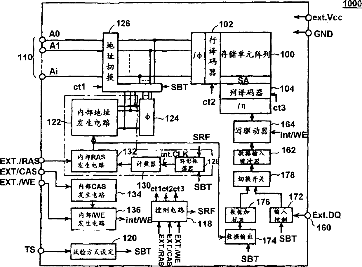
[0107] FIG. 1 is a schematic block diagram showing the structure of a semiconductor memory 1000 according to Embodiment 1 of the present invention.

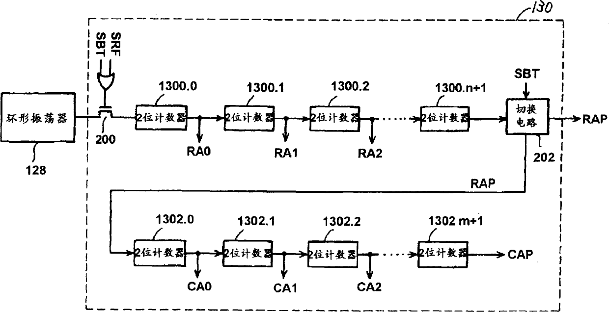
[0108] With reference to Fig. 1, semiconductor memory 1000 comprises: Receive external control signal EXT. / WE, EXT / RAS and EXT / CAS to generate the control circuit 118 of various internal control signals; Under the control of the control circuit 118, the internal row address generation circuit 122 that generates the internal row address signal, the internal row address signal specifies the selected row during the update operation or the burn-in test operation; receives the output of the internal row address generation circuit 122, The arithmetic circuit 124 that performs calculation φ and outputs; the address switching circuit 126, which receives the external address signals Ao~Ai provided by the address signal input terminal 110, the output of the internal row address generation circuit 122, and The output of the arithmetic circu...

Embodiment 2

[0191] Fig. 21 is a circuit diagram showing the configuration of the test mode setting circuit 121 in the second embodiment of the present invention.

[0192] The difference from the configuration of the semiconductor memory 1000 of the first embodiment is that the power supply potential can be supplied to the internal circuit through the test mode signal input terminal in addition to the external power supply potential input terminal.

[0193] The test mode setting circuit 121 includes: a high resistance element R1 connected to the test mode signal input terminal and the ground potential GND; connected to a transistor TD arranged between the test mode input terminal and the ground potential; and connected to the test mode signal Diode D1 between the input terminal and the power supply line.

[0194] By providing a potential greater than the external power supply potential ext.Vcc to the test mode signal input terminal, the signal SBT becomes the "H" level of the active state;...

Embodiment 3

[0204] Fig. 24 is a plan view showing the structure of a semiconductor memory device according to Embodiment 3 of the present invention when it is formed on a wafer.

[0205] In FIG. 24, for semiconductor memory chips arranged two-dimensionally in a wafer, wirings for supplying power supply potential and ground potential are provided in the dicing portion, which is a margin area when these chips are separated by a dicing tool.

[0206] That is, in the semiconductor memory device of Embodiment 3, before the chips are separated in the wafer state, the bonding pad 400 for power supply potential supply and the ground potential supply are provided on the dissociation facet (facet) on the wafer surface, for example. The bonding pad 402 is used. The wiring for supplying the power supply potential to each chip is provided from the power supply potential supply pad through the dicing portion existing between each chip, and similarly, the wiring for supplying the ground potential is pro...


PUM


Abstract

To provide a semiconductor memory capable of shortening the test time and performing a burn-in test in a wafer state regardless of the configuration of a memory cell array. Ring oscillator 128 is activated by external burn-in test designation signal SBT, and the row address signal output from internal row address generation circuit 122 based on the output is supplied to row decoder 102 after being scrambled by arithmetic circuit 124 . On the other hand, the signal output from the data output circuit 174 is scrambled by the data scrambler 176 according to the activation of the signal SBT, and the data of the check structure corresponding to the physical address of the memory cell array is provided to the memory cell array.

Description

technical field [0001] The present invention relates to a semiconductor memory, and more particularly to a semiconductor memory capable of high-speed semiconductor memory testing. Background technique [0002] Accompanying the increase in storage capacity in semiconductor memories, especially dynamic RAM (hereinafter, referred to as DRAM), the time required for semiconductor memory testing has also rapidly increased. [0003] The reason for this problem is that as the storage capacity of the semiconductor memory increases, the number of word lines included in the semiconductor memory increases. Therefore, writing and reading of memory cell information is performed while the word lines are sequentially selected. The working hours become very long. [0004] The above-mentioned problems are particularly severe in burn-in tests and the like. In this burn-in test, the semiconductor memory is operated under high-temperature and high-voltage conditions, so that the performance of...

Claims


Application Information

Patent Timeline
Patent Type & Authority Patents(China)
IPC IPC(8): G01R31/28G11C11/401G11C29/06G11C29/10G11C29/30G11C29/36G11C29/46G11C29/50H01L21/301H01L21/66H01L21/822H01L21/8242H01L27/04H01L27/108
CPCG11C11/401G11C29/30G11C29/36G11C29/46G11C29/50H01L22/00
Inventor 山崎恭治池田丰
Owner MITSUBISHI ELECTRIC CORP
Why Eureka
Try Eureka