Supercharge Your Innovation With Domain-Expert AI Agents!

Manufacturing method of flexible TFT substrate and manufacturing method of flexible OLED panel

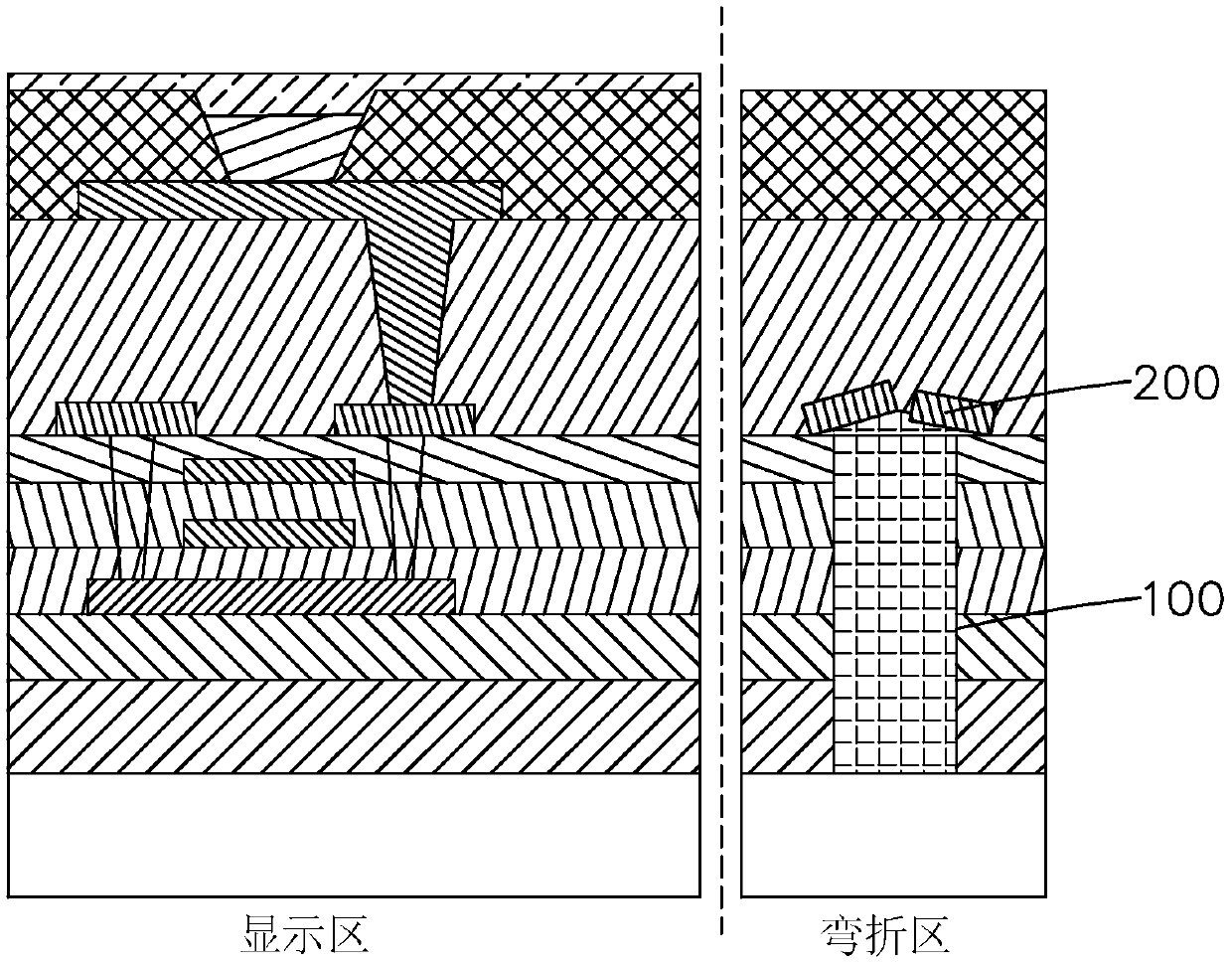
A manufacturing method and a flexible substrate technology, applied in the manufacture of flexible TFT substrates and flexible OLED panels, can solve the problems of SD metal layer 200 fracture, affecting TFT properties, and yield decline, so as to reduce heat and prevent outgassing Phenomenon, the effect of improving properties

Active Publication Date: 2019-04-16
SHENZHEN CHINA STAR OPTOELECTRONICS TECH CO LTD
View PDF5 Cites 1 Cited by
  • Summary
  • Abstract
  • Description
  • Claims
  • Application Information

AI Technical Summary

Problems solved by technology

[0005] In the manufacturing process of the LTPS-TFT backplane of the traditional flexible OLED panel, such as figure 1 Shown is a schematic structural diagram of an existing flexible OLED panel. In order to enhance the bendability of the flexible TFT backplane, a deep hole (deep hole, DH) 100 will be etched in the bending area (bending area), and then the DH100 The ODH material (organic deep hole material) is filled in the center; however, when the source drain (SD) is fabricated subsequently, the SD metal layer 200 needs to be deposited by physical vapor deposition (Physical Vapor Deposition, PVD), because the sputtering chamber The indoor temperature is relatively high, about 220°C-230°C, and the sputtering power is about 40-50kw. During the process of slowly depositing the SD metal layer 200, the heat will slowly accumulate, and the accumulated heat will make the ODH in the lower DH100 Outgassing occurs in the material, which eventually causes the SD metal layer 200 above it to break or even fall off, which seriously affects the properties of the TFT and reduces the yield.

Method used


Image

  • Manufacturing method of flexible TFT substrate and manufacturing method of flexible OLED panel
  • Manufacturing method of flexible TFT substrate and manufacturing method of flexible OLED panel
  • Manufacturing method of flexible TFT substrate and manufacturing method of flexible OLED panel

Examples


Embodiment Construction

[0033] In order to further illustrate the technical means adopted by the present invention and its effects, the following describes in detail in conjunction with preferred embodiments of the present invention and accompanying drawings.

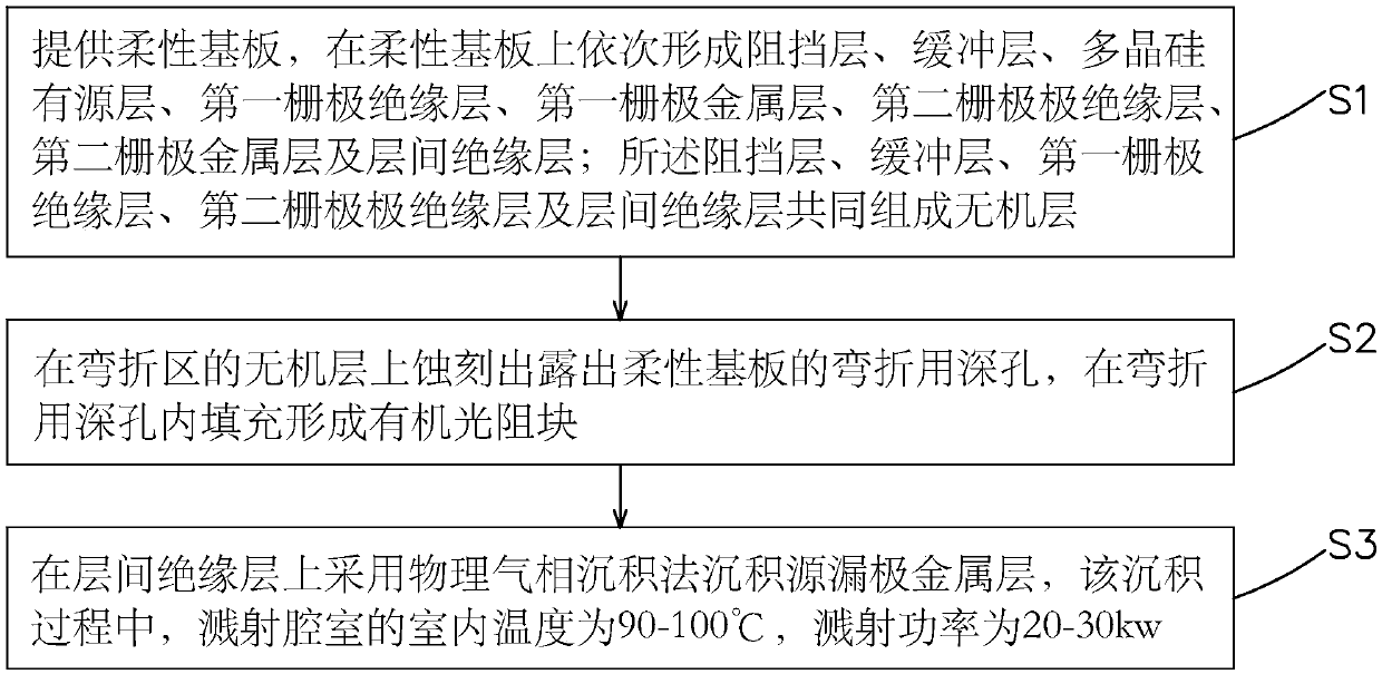
[0034] see figure 2 , the present invention firstly provides a kind of manufacturing method of flexible TFT substrate, comprises the following steps:

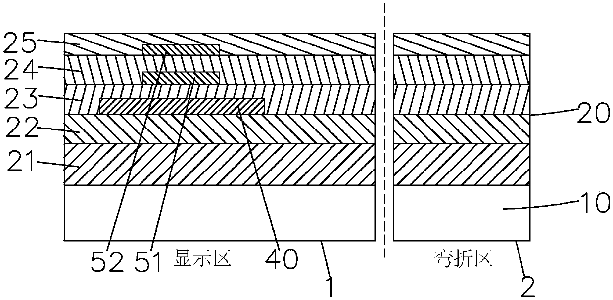
[0035] Step S1, such as image 3 As shown, a flexible substrate 10 is provided, and a barrier layer 21 and a buffer layer 22 of inorganic non-metallic materials are sequentially deposited on the flexible substrate 10, a polysilicon active layer 40 is formed on the buffer layer 22, and a polysilicon active layer 40 is formed on the buffer layer. 22 and the polysilicon active layer 40 are deposited to form a first gate insulating layer 23 of inorganic non-metallic material, deposited and patterned on the first gate insulating layer 23 to form a first gate metal layer 51, in the The second gate...


PUM


Abstract

The invention provides a manufacturing method of a flexible TFT substrate and a manufacturing method of a flexible OLED panel. According to the manufacturing method of the flexible TFT substrate, a source and drain electrode metal layer is deposited and formed by sputtering corresponding elements through a physical vapor deposition (PVD) method, and in the process of depositing the source and drain electrode metal layer through the PVD method, the indoor temperature of a sputtering cavity is 90-100 DEG C; and sputtering power is 20-30 kw. Compared with the prior art, the method has the advantages that the cost is low; the indoor temperature and the sputtering power of the sputtering chamber are reduced during deposition of the source and drain metal layer through the PVD method; therefore,heat accumulated by an organic photoresist block in a deep hole for bending in the process of depositing the source and drain electrode metal layer is reduced, the organic photoresist block in the deep hole for bending can be prevented from deflating, the risk that the source and drain electrode metal layer is broken and falls off at the position is reduced, the property of the flexible TFT substrate is greatly improved, and the product yield is improved.

Description

technical field [0001] The invention relates to the field of display technology, in particular to a method for manufacturing a flexible TFT substrate and a method for manufacturing a flexible OLED panel. Background technique [0002] In the field of display technology, flat panel display devices such as Liquid Crystal Display (LCD) and Active Matrix Organic Light-Emitting Diode (AMOLED) display have thin body, high image quality, Many advantages such as power saving and no radiation have been widely used, such as mobile phones, personal digital assistants (PDAs), digital cameras, computer screens or notebook screens, etc. [0003] Thin Film Transistor (Thin Film Transistor, TFT) array (Array) substrate is the main component of current LCD devices and AMOLED devices, directly related to the development direction of high-performance flat panel display devices, used to provide drive circuits for displays, usually equipped with several A gate scanning line and several data line...

Claims


Application Information

Patent Timeline
IPC IPC(8): H01L27/12H01L21/285H01L21/77C23C14/34C23C14/18C23C14/04
CPCC23C14/04C23C14/18C23C14/34H01L21/2855H01L27/1248H01L27/1259
Inventor 张卜芳李松杉
Owner SHENZHEN CHINA STAR OPTOELECTRONICS TECH CO LTD
Features
  • R&D
  • Intellectual Property
  • Life Sciences
  • Materials
  • Tech Scout
  • Unparalleled Data Quality
  • Higher Quality Content
  • 60% Fewer Hallucinations
Learn More