Copper indium gallium selenium absorption layer prepared by non-vacuum method without selenizing process

A copper indium gallium selenide, non-vacuum technology, applied in the fields of final product manufacturing, sustainable manufacturing/processing, photovoltaic power generation, etc., can solve problems such as toxicity and complex process hazards, achieve mild reaction, stable film structure, and low cost Effect

Active Publication Date: 2019-04-23
HARBIN UNIV OF SCI & TECH
View PDF5 Cites 3 Cited by
  • Summary
  • Abstract
  • Description
  • Claims
  • Application Information

AI Technical Summary

Problems solved by technology

However, in the liquid phase preparation, represented by hydrazine and oleylamine, there is a certain toxicity, and at the same time, there is a certain complexity and danger in the post-selenization process of adding selenium sources. Therefore, it is necessary to find a simple preparation process. Environmental protection, non-toxic preparation process

Method used


Image

  • Copper indium gallium selenium absorption layer prepared by non-vacuum method without selenizing process
  • Copper indium gallium selenium absorption layer prepared by non-vacuum method without selenizing process
  • Copper indium gallium selenium absorption layer prepared by non-vacuum method without selenizing process

Examples


specific Embodiment approach 1

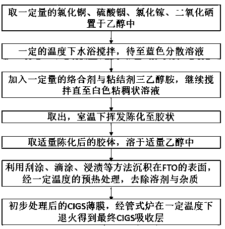
[0017] Specific embodiment 1, a copper indium gallium selenium absorption layer prepared by a non-vacuum method in the non-selenization process of the present invention is carried out according to the following steps:

[0018] One, the preparation of copper indium gallium selenide colloid: take copper chloride, indium sulfate, gallium chloride, selenium dioxide as Cu source, In source, Ga source, Se source, according to (Cu:In:Ga:Se=1: 1.4:0.6:4) molar ratio dissolving in ethanol solvent, adding triethanolamine as a complexing agent and binder, stirring in a water bath at a certain temperature (40-70°C) to a white solution, volatilizing and aging to white at room temperature gelatinous, ready to use;

[0019] 2. Preparation of copper indium gallium selenide precursor thin film: take an appropriate amount of colloid and dissolve it in ethanol, apply it on the substrate by scrape coating method or drop coating method, and remove the solvent and impurities through preliminary hea...

specific Embodiment approach 2

[0021] Embodiment 2: This embodiment differs from Embodiment 1 in that the substrate described in step 2 is fluorine-doped tin dioxide conductive glass, copper sheet, and steel sheet.

specific Embodiment approach 3

[0022] Embodiment 3: This embodiment differs from Embodiment 1 or Embodiment 2 in that: the colloidal thickness of the coating film in the preparation of the CIGS precursor film described in step 2 is 25-95 μm.


PUM


Abstract

The invention relates to a copper indium gallium selenium absorption layer prepared by a non-vacuum method without a selenizing process. The non-vacuum method is characterized by comprising the threetechnological steps of: preparing copper indium gallium selenium colloid, preparing a copper indium gallium selenium precursor film and performing annealing heat treatment. Copper chloride, indium sulfate, gallium chloride and selenium dioxide are utilized as a Cu source, an In source, a Ga source and an Se source and are prepared according to the molar ratio (Cu to In to Ga to Se = 1 to 1.4 to 0.6 to 4); ethyl alcohol is utilized as a solvent; triethanolamine is simultaneously added into to serve as a complexing agent and an adhesive; the materials are stirred for dissolving under a certain temperature until white thick liquid is obtained; the white thick liquid is taken out, volatilized and aged; the white thick liquid is moderately dissolved into the ethyl alcohol and then scrape coatedor dispensed to a substrate; the copper indium gallium selenium absorption layer is obtained after certain-temperature heat treatment. The copper indium gallium selenium absorption layer disclosed bythe invention has the advantages of simple production technology and environmental protection; a flat copper indium gallium selenium film with a completed structure and a forbidden bandwidth of 1.39eV can be obtained without through any refeeding selenizing technology.

Description

technical field [0001] The invention relates to the field of new energy sources of optoelectronic materials, in particular to a copper indium gallium selenium absorbing layer prepared by a non-vacuum method without selenization process. Background technique [0002] Energy is an important material basis for the existence and development of human civilization. With the rapid development of social economy, the increasingly serious environmental pollution problems and the continuous increase in energy demand, traditional energy represented by fossil energy such as coal, oil and natural gas can no longer meet the needs of social and economic development. Therefore, all countries in the world regard the development of new energy and renewable and sustainable energy as an important way to solve energy and environmental problems. Photovoltaic power generation directly converts solar energy into electricity, providing a practical and sustainable solution to the growing global energ...

Claims


Application Information

Patent Timeline
Patent Type & Authority Applications(China)
IPC IPC(8): H01L31/032H01L31/18
CPCH01L31/0322H01L31/18Y02E10/541Y02P70/50
Inventor 李丽波翟墨杜金田谢明
Owner HARBIN UNIV OF SCI & TECH
Why Eureka
Try Eureka