

High-reflection film layer for laser device resistant to high temperature and strong acid corrosion in waste gas, and preparation method of high-reflection film layer
A laser device and high-reflection film technology, applied in coating, sputtering, metal material coating processes, etc., can solve the problems of poor bonding force and difficult thickness control, and achieve the effect of stable performance and strong bonding force
- Summary
- Abstract
- Description
- Claims
- Application Information
AI Technical Summary
Problems solved by technology
Method used
Image

Examples
preparation example Construction
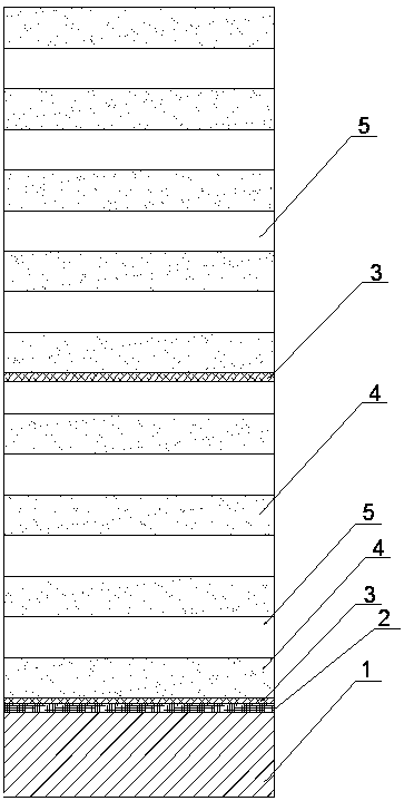
[0043] The above-mentioned preparation method of the high-reflection film layer for laser devices with high temperature resistance and strong acid corrosion resistance in exhaust gas, the specific steps are as follows:
[0044] 1) Substrate preparation: polishing substrate;
[0045] 2) Magnetron sputtering Ti film: Ti film is plated on the surface of the Ti alloy substrate;
[0046] 3) Coating Ag film: Coating Ag film with reflective film on the Ti film;
[0047] 4) TiO plating 2 Film: Ag film is coated with high transmission film TiO 2 membrane;
[0048] 5) Plating SiO 2 Film: on TiO 2 Coated with high-reflection film SiO 2 membrane;
[0049] 6) Alternate coating: TiO 2 Membrane and SiO 2 The films alternated for 8 cycles, at the end of the 4th cycle, the SiO 2 Ag film is plated on the film, and TiO is plated on the Ag film 2 Film, TiO 2 SiO plating on the film 2 Membranes...alternate the remaining 4 cycles, at the last layer of SiO 2 Re-coating TiO on the film ...
Embodiment 1
[0063] A high-reflection film layer for laser devices with high temperature resistance and strong acid corrosion resistance in exhaust gas, comprising a substrate, a Ti film is plated on the substrate, an Ag film is plated on the Ti film, and TiO is plated on the Ag film 2 Film, TiO 2 SiO plating on the film 2 Membrane, SiO 2 TiO plated on film 2 Film, TiO 2 Membrane and SiO 2 The films alternated for 4 cycles, at the end of the 4th cycle, the SiO 2 Ag film is plated on the film, and TiO is plated on the Ag film 2 Film, TiO 2 SiO plating on the film 2 film... 4 more cycles alternated, at the last layer of SiO 2 Re-coating TiO on the film 2 film to prepare a high-reflection film layer for laser devices.
[0064] The matrix is Ti-6Al-4V alloy.
[0065] The thickness of the Ti film is 20nm, the Ag film, TiO 2 Membranes and SiO 2 The film thicknesses were all 500 nm.
[0066] The thickness of the substrate is 500 μm.
[0067] The above-mentioned preparation method...
Embodiment 2
[0078] A high-reflection film layer for laser devices with high temperature resistance and strong acid corrosion resistance in exhaust gas, comprising a substrate, a Ti film is plated on the substrate, an Ag film is plated on the Ti film, and TiO is plated on the Ag film 2 Film, TiO 2 SiO plating on the film 2 Membrane, SiO 2 TiO plated on film 2 Film, TiO 2 Membrane and SiO 2 The films alternated for 4 cycles, at the end of the 4th cycle, the SiO 2 Ag film is plated on the film, and TiO is plated on the Ag film 2 Film, TiO 2 SiO plating on the film 2 film... 4 more cycles alternated, at the last layer of SiO 2 Re-coating TiO on the film 2 film to prepare a high-reflection film layer for laser devices.
[0079] The matrix is Ti-6Al-4V alloy.
[0080] The thickness of the Ti film is 22 nm, the thickness of the Ag film is 620 nm, and the thickness of the TiO film is 22 nm. 2 The thickness of the film is 550 nm, SiO 2 The thickness of the film was 600 nm.
[0081]...
PUM
| Property | Measurement | Unit |
|---|---|---|
| thickness | aaaaa | aaaaa |
| thickness | aaaaa | aaaaa |
| thickness | aaaaa | aaaaa |
Abstract
Description
Claims
Application Information