Schottky diode structure and manufacturing method thereof

A technology of Schottky diode and manufacturing method, which is applied in semiconductor/solid-state device manufacturing, electrical components, circuits, etc., can solve problems such as weakening reverse voltage withstand capability, reducing forward conduction current of devices, and increasing on-resistance.

Inactive Publication Date: 2019-05-10
安徽长飞先进半导体有限公司
View PDF4 Cites 8 Cited by
  • Summary
  • Abstract
  • Description
  • Claims
  • Application Information

AI Technical Summary

Problems solved by technology

[0006] 1. The JBS structure introduces p in the drift region + area, in the case of low voltage, the conduction current is mainly done by the Schottky, P + The introduction of the area will reduce the forward conduction current of the device and increase the on-resistance; however, increasing the Schottky area improves the forward conduction characteristics and at the same time we

Method used


Image

  • Schottky diode structure and manufacturing method thereof
  • Schottky diode structure and manufacturing method thereof

Examples


Embodiment Construction

[0054] Referring to the accompanying drawings, through the description of the embodiments, the specific embodiments of the present invention include the shape, structure, mutual position and connection relationship of each part, the function and working principle of each part, and the manufacturing process of the various components involved. And the method of operation and use, etc., are described in further detail to help those skilled in the art have a more complete, accurate and in-depth understanding of the inventive concepts and technical solutions of the present invention.

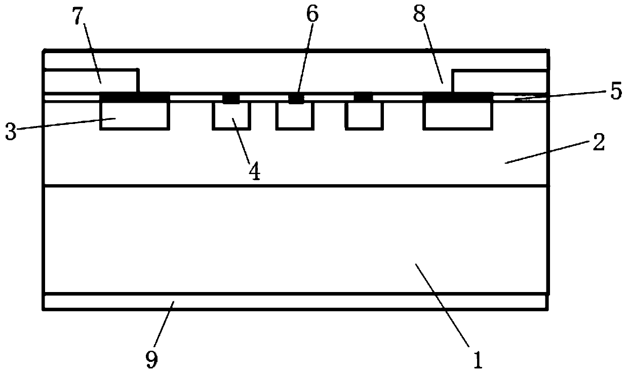
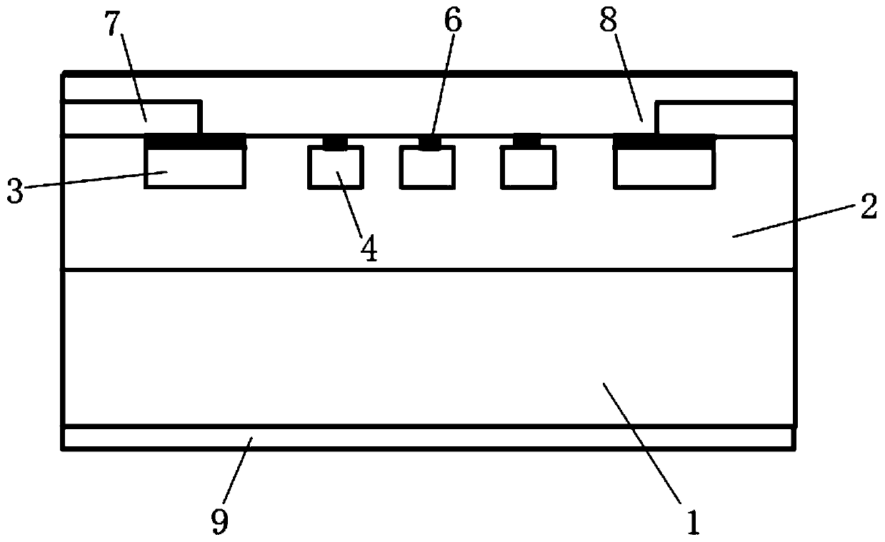
[0055] Such as figure 1 , 2 As shown, the junction barrier Schottky diode has a substrate, the substrate N type 4H-SiC type substrate, such as N + SiC substrate 1, the upper surface of the substrate is N - The first drift layer of conductivity type, such as N can be grown by CVD - SiC epitaxial layer 2 as the first drift layer, N - The thickness of SiC epitaxial layer 2 is 5um-100um, and the dopi...


PUM

PropertyMeasurementUnit
Thicknessaaaaaaaaaa
Thicknessaaaaaaaaaa
Thicknessaaaaaaaaaa

Abstract

The invention discloses a junction barrier schottky diode. An N-conductive type first drift layer is arranged on the upper surface of a substrate; back surface ohmic contact metal is arranged on the lower surface of the substrate; a p+ ion injection region is formed on the upper surface of the first drift layer through ion injection; front surface schottky contact metal is on the first drift layerand the upper surface of the p+ ion injection region; an N-conductive type second drift layer is between the first drift layer and the front surface schottky contact metal; and a P++ injection regionis between the p+ ion injection region and the front surface schottky contact metal. According to the diode disclosed by the invention, after JTE and FLR are finished, an N-Sic epitaxial layer is manufactured on the upper surface, and the small-area P++ region is prepared through the N-epitaxial layer, so that the contact area of the schottky metal is enlarged, the forward current density is increased, and meanwhile, no influence is caused on the aspect of reverse voltage withstand; and in addition, the P type region in the N-SiC epitaxial layer is heavily doped, so that peak current can be increased, and the surge resistance of a device can be improved.

Description

technical field [0001] The invention relates to a junction barrier Schottky diode structure and a manufacturing process thereof. Background technique [0002] Compared with the first-generation semiconductor and the second-generation semiconductor, SiC material has the advantages of large band gap, high breakdown electric field, saturation drift speed and thermal conductivity, etc., and is widely used in the preparation of high temperature, high frequency, radiation resistance, High-power electronic devices and power electronic devices made of SiC materials have become a frontier research field in the field of semiconductors. [0003] JBS (junction barrier schottky, junction barrier Schottky diode) combines the high withstand voltage and low leakage current of PiN diodes and the ground conduction characteristics of Schottky diodes, and combines SiC materials with JBS structures to prepare SiC. JBS structures integrate SiC The electrical performance advantages of the materia...

Claims


Application Information

Patent Timeline
IPC IPC(8): H01L29/06H01L21/329H01L29/872
Inventor 史田超宋东波程海英赵海明史文华钟敏刘锦锦
Owner 安徽长飞先进半导体有限公司
Why Eureka
Try Eureka