A kind of soi structure and its manufacturing process

A manufacturing process and technology of silicon wafers, applied in the fields of semiconductor/solid-state device manufacturing, semiconductor/solid-state device components, semiconductor devices, etc., can solve problems such as poor heat dissipation of SOI, improve heat dissipation performance, improve heat dissipation capacity, and inhibit self-heating effect of effect

Active Publication Date: 2020-10-16
ZHEJIANG UNIV
View PDF4 Cites 0 Cited by
  • Summary
  • Abstract
  • Description
  • Claims
  • Application Information

AI Technical Summary

Problems solved by technology

It is an effective method to solve the poor heat dissipation of SOI by using insulating materials with high thermal conductivity instead of silicon dioxide without affecting the interfacial properties of the thin film interface.

Method used


Image

  • A kind of soi structure and its manufacturing process
  • A kind of soi structure and its manufacturing process
  • A kind of soi structure and its manufacturing process

Examples


Embodiment

[0036] Manufacturing process of the present invention comprises the following steps:

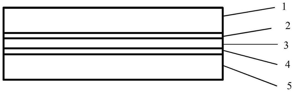
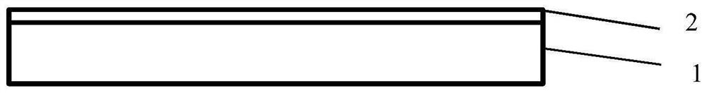
[0037] 1) if figure 2 As shown, a layer of about 10nm silicon dioxide film is sputtered on the surface of the first silicon wafer layer 1 by radio frequency sputtering as the silicon dioxide layer 2;

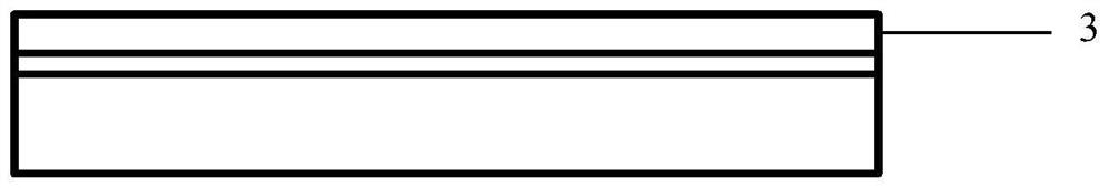
[0038] 2) if image 3 As shown, a layer of boron nitride film with a thickness of about 700 nm is sputtered on the surface of the silicon dioxide layer 2 in step 1 as the boron nitride layer 3;

[0039] 3) if Figure 4 As shown, a layer of silicon with a thickness of about 1 μm is sputtered on the surface of the boron nitride layer 3 in step 2 as the silicon layer 4;

[0040] 4) if Figure 5 As shown, the surface of the silicon layer 4 obtained in step 3 is polished by chemical mechanical polishing, and then the polished silicon layer 4 is thermally bonded to the second silicon wafer layer 5 to obtain an inverted SOI structure;

[0041] 5) if Figure 6 As shown, the inverted SOI structu...


PUM

PropertyMeasurementUnit
thicknessaaaaaaaaaa
thicknessaaaaaaaaaa
thicknessaaaaaaaaaa

Abstract

The invention discloses a novel SOI structure and a manufacturing technology thereof. The novel SOI structure comprises a top silicon layer, an insulation layer and a back substrate arranged successively from top to bottom, and is characterized in that the insulation layer is mainly formed by a silicon dioxide layer and boron nitride layer combined double-layer composite structure, the top siliconlayer comprises a first silicon chip layer, the back substrate is mainly formed by thermal bonding of a sputtered silicon layer to a second silicon chip layer, the first silicon chip layer is arranged in the upper surface of the silicon dioxide layer, and the silicon layer is arranged in the lower surface of the boron nitride layer. The heat radiation performance of a traditional SOI structure isimproved, the heat radiation capability of the insulation layer is improved without influence on the insulation performance, and further the heat radiation performance based on the SOI device is improved.

Description

technical field [0001] The invention relates to the technical field of semiconductor SOI, in particular to an SOI structure with better heat dissipation performance and a manufacturing process thereof. Background technique [0002] SOI (Silicon-On-Insulator, silicon on insulating substrate) technology introduces an insulating layer between the top silicon and the back substrate. By forming a semiconductor thin film on an insulator, the SOI material has the incomparable advantages of bulk silicon: it can realize the dielectric isolation of components in integrated circuits, and completely eliminate the parasitic latch effect in bulk silicon CMOS circuits; The integrated circuit also has the advantages of small parasitic capacitance, high integration density, fast speed, simple process, small short channel effect, and is especially suitable for low-voltage and low-power circuits. Therefore, it can be said that SOI will likely become a deep submicron low-voltage , The mainstre...

Claims


Application Information

Patent Timeline
Patent Type & Authority Patents(China)
IPC IPC(8): H01L27/12H01L21/20H01L21/762H01L21/84H01L23/367
Inventor 张亮汪小知吴永志骆季奎杨杭生曾翔宇沃华雷李威李梦露
Owner ZHEJIANG UNIV
Why Eureka
Try Eureka