3D NAND memory array common source forming method

A 3D NAND and memory technology, which is applied in the direction of electric solid-state devices, semiconductor devices, electrical components, etc., can solve the problems of photolithography deformation, complicated steps, and device performance degradation, etc., to prevent etching damage, high etching selectivity, and simplify The effect of the production process

Inactive Publication Date: 2019-06-07
YANGTZE MEMORY TECH CO LTD
View PDF12 Cites 8 Cited by
  • Summary
  • Abstract
  • Description
  • Claims
  • Application Information

AI Technical Summary

Problems solved by technology

[0004] Among them, the Array Common Source (ACS for short) is an important structure requiring high conductivity. Currently, there are many schemes for forming the Array Common Source. In the first scheme, ACS is usually filled with tungsten (W). , although tungsten has good electrical conductivity, in the process of its formation, due to the large stress, it will cause various process problems, such as wafer warping and sliding, photolithography deformation, stacking dislocation, etc., which will lead to device performance degradation of
Therefore, in the second solution, polysilicon is used to replace tungsten, but the conductivity of polysilicon is much lower than that of tungsten. Even if doped polysilicon is used, its conductivity is still much lower than that of tungsten, and the production cost is relatively high.
[0005] The third solution takes both stress and resistance into account. This solution is to form the common source of the array by forming polysilicon and metal plugs on the polysilicon. However, the steps for forming the common source of the array in this solution are more complicated and increase the process cost

Method used


Image

  • 3D NAND memory array common source forming method
  • 3D NAND memory array common source forming method
  • 3D NAND memory array common source forming method

Examples


Embodiment Construction

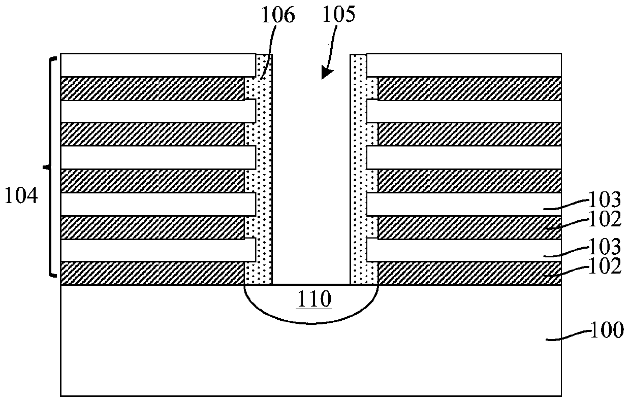
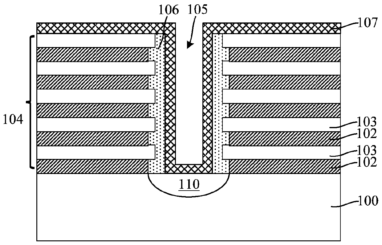
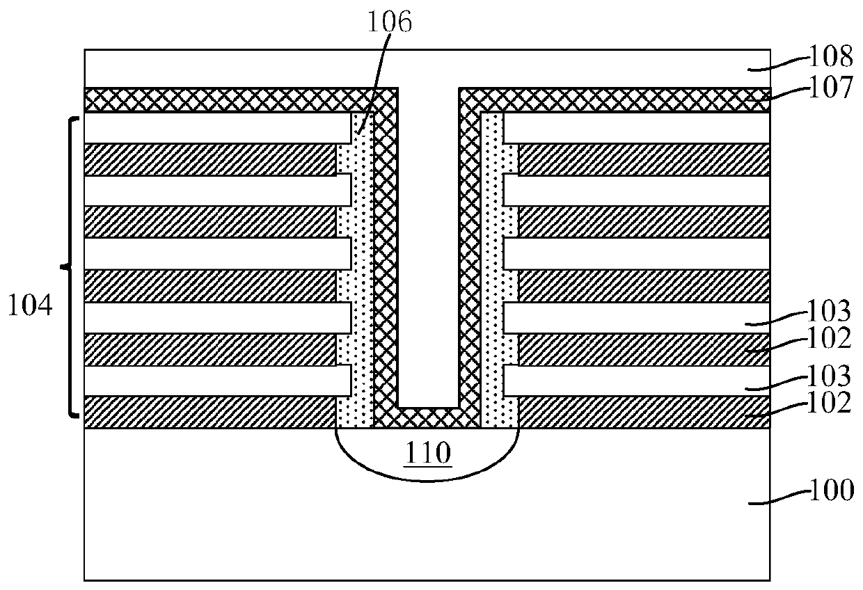
[0027] As mentioned in the background art, the existing steps of forming the array common source are relatively complicated, which increases the process cost.

[0028] It is found that the existing steps of forming the common source of the array include: providing a stack structure in which the control gate and the isolation layer are stacked on each other, and a gate spacer is formed in the stack structure; forming polysilicon on the surface of the gate spacer and the stack structure layer; then planarize (chemical mechanical polishing, CMP) the polysilicon layer until the surface of the stack structure is exposed; after the planarization step, etch back to remove the polysilicon layer with a partial thickness in the gate spacer; the polysilicon layer after etch back The surface of the layer is filled with metal to form a metal plug. The aforementioned steps of forming the common source of the array are relatively complicated, which increases the process cost.

[0029] For t...


PUM


Abstract

The invention discloses a 3D NAND memory array common source forming method. The method comprises steps: a substrate is provided, wherein a stacked structure is formed on the substrate, and a gate separation slot exposing the surface of the substrate is formed in the stacked structure; metal contact layers are formed on the surface of the side wall and the bottom of the gate separation slot and the surface of the stacked structure; a polysilicon layer covering the metal contact layer is formed, wherein the polysilicon layer fills the gate separation slot; the polysilicon layer with a partial thickness in the gate separation slot is etched back and removed, and the metal contact layer is used as an etching stop layer; and a metal plug is formed on the etched polysilicon layer. The array common source forming process is simplified.

Description

technical field [0001] The invention relates to the field of semiconductor manufacturing, in particular to a method for forming an array common source of a 3D NAND memory. Background technique [0002] NAND flash memory is a better storage device than hard disk drives, and it has been widely used in electronic products as people pursue non-volatile storage products with low power consumption, light weight and high performance. At present, the planar NAND flash memory is close to the limit of practical expansion. In order to further increase the storage capacity and reduce the storage cost per bit, a 3D NAND memory is proposed. [0003] At present, the main components of 3D NAND memory can include array storage units and peripheral circuits, and the data access operations in each storage unit are realized through the control of peripheral circuits. Therefore, in the manufacturing process of 3D NAND memory, the conductance of each part Rate is an important link that cannot be...

Claims


Application Information

Patent Timeline
Patent Type & Authority Applications(China)
IPC IPC(8): H01L21/28H01L27/1157H01L27/11578H01L29/417
Inventor 袁野刘淼程强任连娟郭玉芳王玉岐
Owner YANGTZE MEMORY TECH CO LTD
Why Eureka
Try Eureka