
LED epitaxial structure and preparation method thereof, and LED chip

An epitaxial structure, N-type technology, applied in the direction of electrical components, circuits, semiconductor devices, etc., can solve the problems of low hole and electron recombination rate, carrier imbalance, limiting the improvement of LED luminous efficiency, etc., to achieve improved recombination efficiency, increase the effective area, and improve the effect of LED luminous efficiency

Inactive Publication Date: 2019-06-07
ENRAYTEK OPTOELECTRONICS
View PDF6 Cites 11 Cited by
  • Summary
  • Abstract
  • Description
  • Claims
  • Application Information

AI Technical Summary

Problems solved by technology

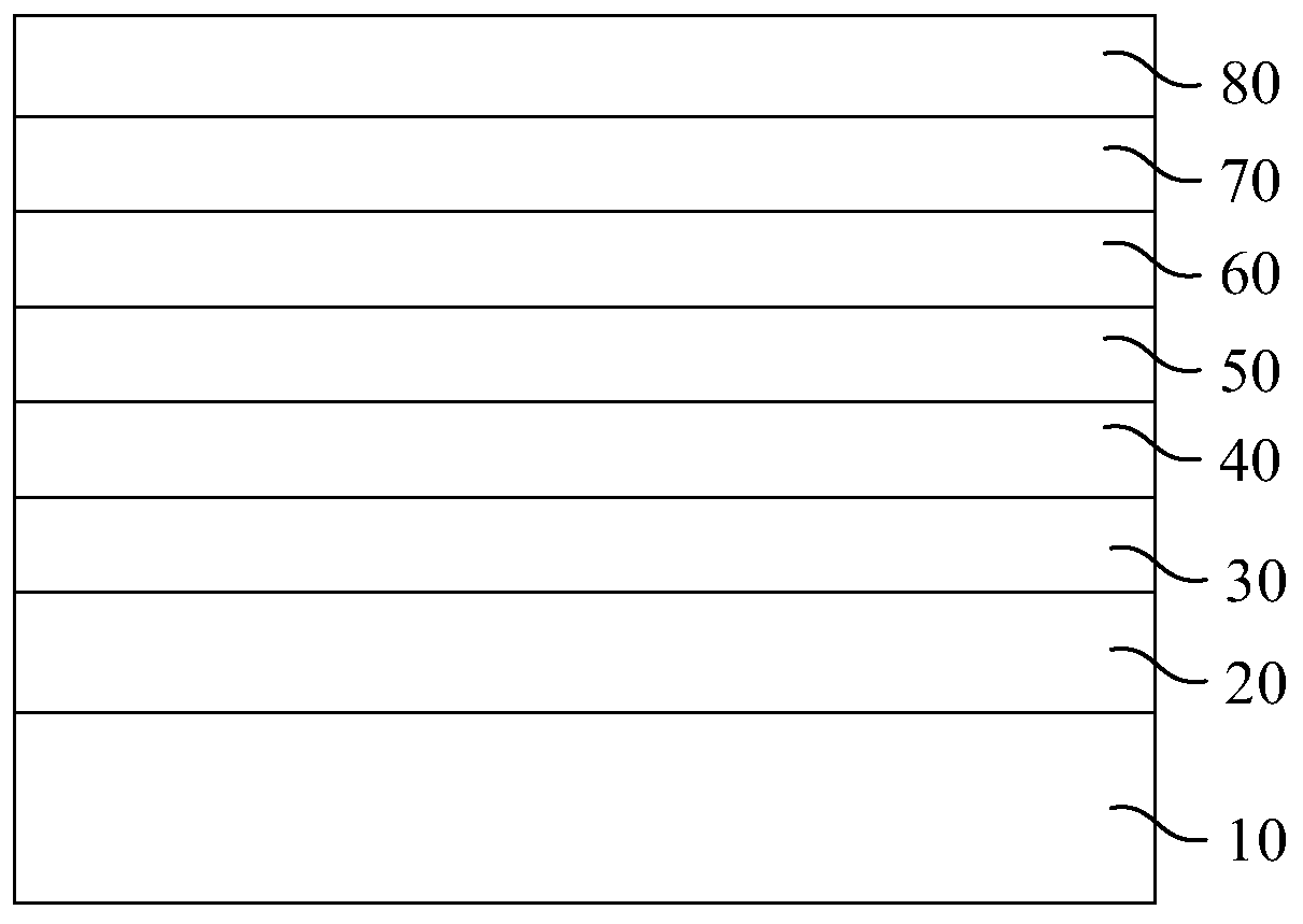
And in the LED hole mobility rate (about 10cm 2 / Vs) is much lower than the electron mobility (about 300cm 2 / Vs), so, in the LED, the problem of unbalanced majority carriers on the side of the multi-quantum well layer 60 near the N-type GaN layer 40 and the side of the multi-quantum well layer 60 near the P-type GaN layer 80 is likely to occur, so that The recombination rate of holes and electrons is low, which seriously limits the improvement of LED luminous efficiency

Method used


Image

  • LED epitaxial structure and preparation method thereof, and LED chip
  • LED epitaxial structure and preparation method thereof, and LED chip
  • LED epitaxial structure and preparation method thereof, and LED chip

Examples


preparation example Construction

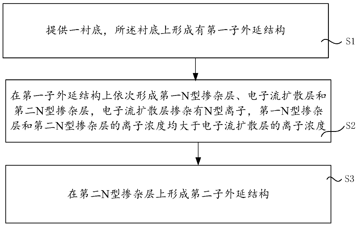
[0040] image 3 It is a schematic flow chart of the method for preparing the LED epitaxial structure in this embodiment. Such as image 3 As shown, this embodiment also provides a method for preparing an LED epitaxial structure, comprising the following steps:

[0041] Step S1: providing a substrate on which a first sub-epitaxial structure is formed;

[0042] Step S2: sequentially forming a first N-type doped layer, an electron flow diffusion layer, and a second N-type doped layer on the first sub-epitaxial structure to form an N-type doped structure, and the electron flow diffusion layer is doped with Doped with N-type ions, the concentration of ions doped in the first N-type doped layer and the second N-type doped layer is greater than the concentration of N-type ions doped in the electron current diffusion layer; and

[0043] Step S3: forming a second sub-epitaxial structure on the second N-type doped layer.


PUM

PropertyMeasurementUnit
Thicknessaaaaaaaaaa
Thicknessaaaaaaaaaa
Thicknessaaaaaaaaaa

Abstract

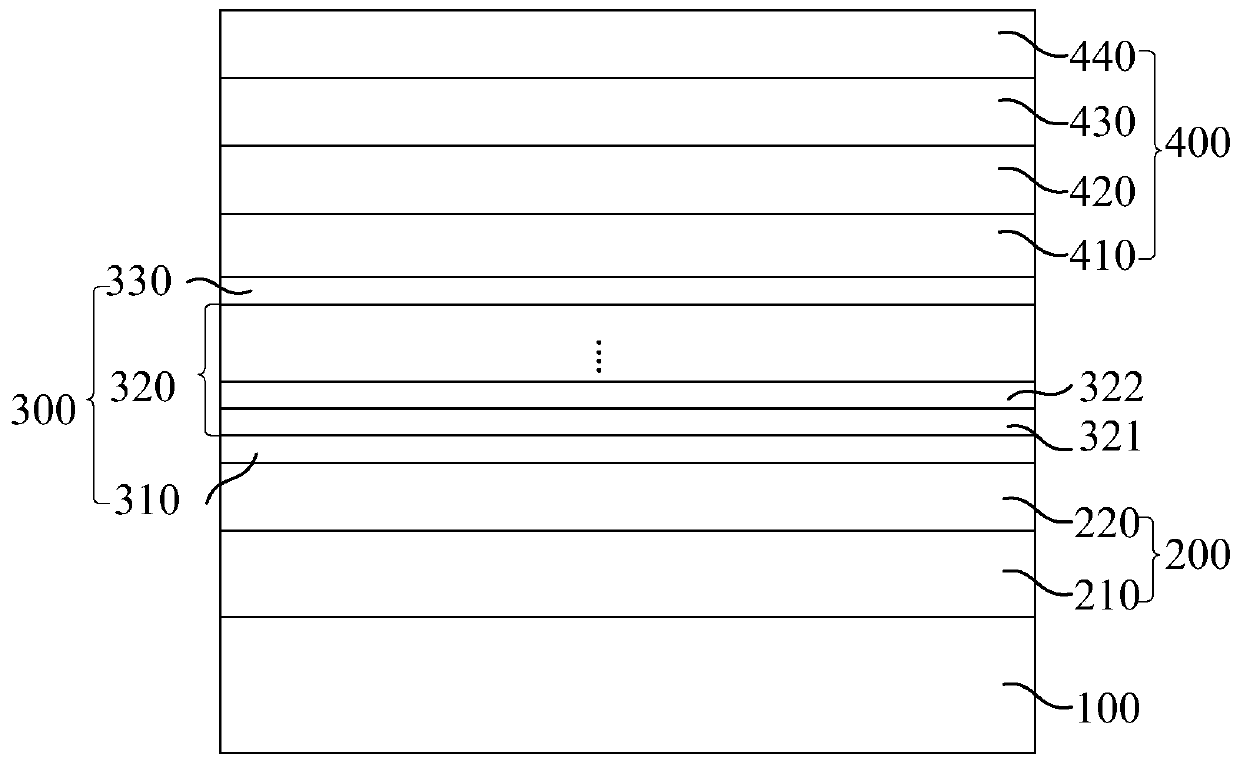
The invention provides an LED epitaxial structure and a preparation method thereof, and an LED chip. The LED epitaxial structure includes a first sub-epitaxial structure, an N-type doping structure and a second sub-epitaxial structure which are successively superposed on a substrate; the N-type doping structure includes a first N-type doping layer, an electron flow diffusion layer and a second N-type doping layer; and the electron flow diffusion layer is doped with N-type ions. The concentrations of the ions doped in the first and second N-type doping layers are greater than that of the N-typeions of the electron flow diffusion layer, so that the electron mobility at the internal of the electron flow diffusion layer can be enhanced, the effective areas of electron migration in the N-typedoping structure can be increased, and therefore, the recombination rates of holes and electrons can be enhanced, and LED luminous efficiency can be enhanced as well.

Description

technical field [0001] The invention relates to the field of semiconductor integrated circuit manufacturing, in particular to an LED epitaxial structure, a preparation method thereof, and an LED chip. Background technique [0002] A light emitting diode (Light Emitting Diode, referred to as LED) is a semiconductor solid-state light-emitting device, which uses a semiconductor P-N junction as a light-emitting material, and can directly convert electrical energy into light energy. Among various semiconductor materials, III-V compound semiconductors represented by gallium nitride (GaN) have the advantages of good heat dissipation, ability to carry large currents, high luminous intensity, low power consumption, and long life, making light-emitting diodes In particular, high-brightness blue light-emitting diodes and white light-emitting diodes are widely used in general lighting, landscape lighting, display backlighting, and automotive lighting. [0003] Such as figure 1 As show...

Claims


Application Information

Patent Timeline
IPC IPC(8): H01L33/14H01L33/00
Inventor 游正璋卢国军
Owner ENRAYTEK OPTOELECTRONICS
Learn More