Infrared transparent conductive film, and preparation method and application thereof

A transparent conductive film, infrared technology, used in cable/conductor manufacturing, conductive layers on insulating carriers, circuits, etc., can solve the problems of image quality, poor performance of multi-layer films, no electromagnetic shielding, etc., and achieve good electrical conductivity. high infrared transmittance, simple preparation process, and high infrared transmittance

Inactive Publication Date: 2019-06-11
SHENZHEN PLANCK INNOVATION TECH CO LTD
View PDF7 Cites 4 Cited by
  • Summary
  • Abstract
  • Description
  • Claims
  • Application Information

AI Technical Summary

Problems solved by technology

[0003] CN105112869B discloses a preparation method of yttrium-doped copper oxide infrared transparent conductive film, in order to solve the problem that the infrared transmittance of the protective cover of the existing infrared detector is low and the frost and fog on the surface will affect the quality of imaging, but It does not have the effect of electromagnetic shielding, and its application range is small
The performance of the multilayer film is poor and cannot meet the requirements of excellent infrared transparent conductive film

Method used


Image

  • Infrared transparent conductive film, and preparation method and application thereof
  • Infrared transparent conductive film, and preparation method and application thereof
  • Infrared transparent conductive film, and preparation method and application thereof

Examples


Embodiment 1

[0072] A kind of preparation method of infrared transparent conductive film comprises the steps:

[0073] (1) Vacuumize the system to a vacuum degree of 2.5×10 -4 Pa, then filled with oxygen to a vacuum of 2.4×10 -2 Pa, with the beam flow of yttrium oxide being 80mA, depositing yttrium oxide on quartz with a thickness of 1mm at 200°C at a rate of 0.4nm / s to obtain a seed layer with a thickness of 50nm;

[0074] (2) annealing the seed layer obtained in step (1) at 500° C. for 2 hours to obtain the annealed seed layer;

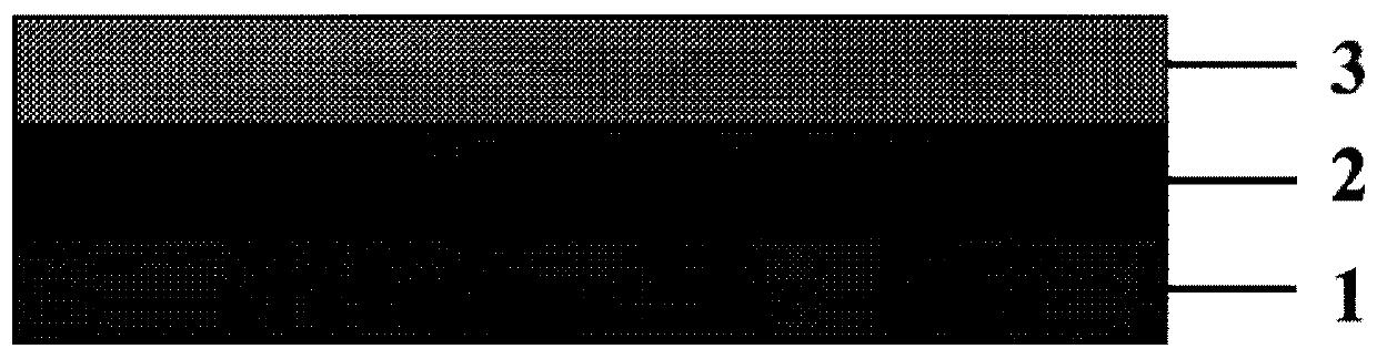
[0075] (3) With the beam current of indium oxide doped with cerium fluoride being 30mA, a conductive layer with a thickness of 150nm was deposited on the annealed seed layer at a speed of 0.2nm / s with indium oxide doped with cerium fluoride, The content of cerium fluoride in the conductive layer is 5 wt%, and then annealed at 300° C. for 1 hour to obtain an infrared transparent conductive film. The structure of the infrared transparent conductive film is as ...

Embodiment 2

[0077] The difference from Example 1 is that the deposition thickness of the seed layer in step (1) is 20 nm.

Embodiment 3

[0079] The difference from Example 1 is that the deposition thickness of the seed layer in step (1) is 300 nm.


PUM

PropertyMeasurementUnit
thicknessaaaaaaaaaa
thicknessaaaaaaaaaa
thicknessaaaaaaaaaa

Abstract

The invention relates to an infrared transparent conductive film, and a preparation method and an application thereof. The infrared transparent conductive film comprises a substrate and a seed layer and a conductive layer sequentially arranged on the substrate; the seed layer is made from material of a square iron ferromanganese ore cubic crystal structure; the conductive layer is an indium oxide-doped IIIB compound. According to the infrared transparent conductive film, and the preparation method and the application thereof, the material of the square iron ferromanganese ore cubic crystal structure is used as the seed layer, the indium oxide-doped IIIB compound is used as the conductive layer, the crystal structure of the seed layer is the same as that of indium oxide, so that the acquired infrared transparent conductive film has the good photoelectric property, compared with the prior art adopting the metal mesh and the ITO film mesh, the infrared transparent conductive film has theadvantages of high film hardness, strong adhesive force and high infrared transmittance.

Description

technical field [0001] The invention belongs to the field of semiconductor material science, and in particular relates to an infrared transparent conductive film, a preparation method and application thereof. Background technique [0002] Transparent conductive films have extensive application value and important research significance in the fields of energy, information, and national defense. As the key electrode material of optoelectronic devices, there is a huge market demand in the fields of flat-panel displays, touch screens and thin-film solar cells. One of the important aspects is to shield electromagnetic interference. With the continuous development of optical technology, more and more optical systems (including visible and infrared optical systems) have put forward clear requirements on the performance of anti-electromagnetic interference, which requires the optical system to increase the function of shielding electromagnetic waves on the basis of the original func...

Claims


Application Information

Patent Timeline
Patent Type & Authority Applications(China)
IPC IPC(8): H01B5/14H01B1/02H01B1/08H01B13/00
Inventor 孙小卫王恺张楠丁时浩徐冰
Owner SHENZHEN PLANCK INNOVATION TECH CO LTD
Why Eureka
Try Eureka