Enhanced transistor based on III oxide passivation and manufacturing method of enhanced transistor

A production method and oxide technology, which is applied in semiconductor/solid-state device manufacturing, semiconductor devices, electrical components, etc., can solve the problems of reducing saturation current and reducing the concentration of two-dimensional electron gas affecting the channel, so as to reduce on-resistance, The effect of optimized processing method and excellent high temperature stability

Inactive Publication Date: 2019-06-21
SUZHOU INST OF NANO TECH & NANO BIONICS CHINESE ACEDEMY OF SCI
View PDF2 Cites 7 Cited by
  • Summary
  • Abstract
  • Description
  • Claims
  • Application Information

AI Technical Summary

Problems solved by technology

This method makes the P-type doped region capping layer and H 2 The plasma reaction forms a high-resistance layer, which avoids the problems of etching uniformity, repeatability and introduction of damage caused by the etching method, but the P-type doped region in the non-gate region lies in the H 2 The high-resistance layer formed by plasma passivation, when the operating temperature of the device exceeds 450 ° C, the high-resistance l...

Method used


Image

  • Enhanced transistor based on III oxide passivation and manufacturing method of enhanced transistor
  • Enhanced transistor based on III oxide passivation and manufacturing method of enhanced transistor
  • Enhanced transistor based on III oxide passivation and manufacturing method of enhanced transistor

Examples


Embodiment Construction

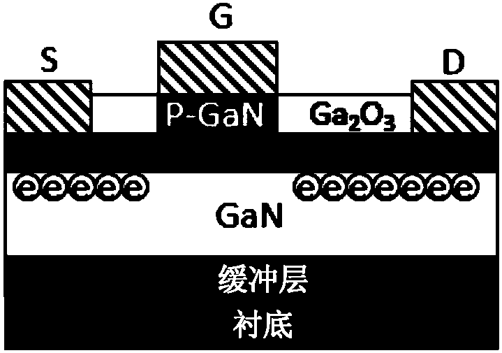
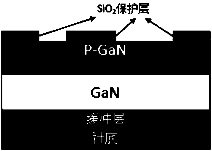
[0054] In view of the deficiencies in the prior art, the inventor of this case has been able to propose the technical solution of the present invention after long-term research and extensive practice, which mainly uses oxidation or other techniques to transform the P-type doped region of the non-gate region into a Ш group oxidation The P-type doped region in the region under the gate is reserved, so as to realize the transistor in the P-type capping layer enhanced mode of operation.

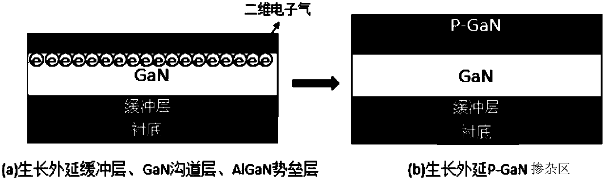
[0055] Specifically, the present invention adopts P-type doped region cap layer / AlGaN barrier layer / GaN channel layer / base (or P-type doped region cap layer / AlGaN barrier layer / AlN / GaN channel layer / base, etc. Similar structure) material structure, the P-type doped region in the non-gate region is changed into a Ш group oxide by oxidation or other methods, the P-type doped region in the region under the gate is retained, and the two-dimensional electron gas of the channel layer is depleted ( 2DEG...


PUM


Abstract

The invention discloses an enhanced transistor based on III oxide passivation and a manufacturing method of the enhanced transistor. The manufacturing method comprises the steps of growing and forminga heterojunction on a substrate, wherein the heterojunction comprises a first semiconductor and a second semiconductor formed on the first semiconductor, the second semiconductor has a band gap whichis wider than the first semiconductor, and two-dimensional electron gas is formed in the heterojunction; forming a cap layer on the second semiconductor, wherein the cap layer comprises a doping region and passivation regions, and the doping region is composed of a third semiconductor and is completely covered by the gate, the passivation regions are distributed between the gate and the drain andbetween the gate and the source, and the third semiconductor is used for exhausting the two-dimensional electron gas distributed in a gate lower region in the heterojunction; and making the source, the drain and the gate. According to the enhanced transistor disclosed by the invention, the uniformity, repeatability and introduction damage problems caused by etching the P-type doping region can beavoided, and the device reliability problem caused by the fact that a high-resistance layer formed by hydrogen plasma passivation is possibly re-activated at a high temperature can be avoided.

Description

technical field [0001] The invention relates to an enhanced transistor, in particular to an enhanced transistor based on Group III oxide passivation and a manufacturing method thereof, belonging to the technical field of semiconductor devices. Background technique [0002] With the rapid development of the economy in today's era, people's awareness of environmental protection and resource conservation is becoming stronger and stronger, requiring lower and lower losses and higher efficiency in the process of energy conversion. In order to achieve this low loss and high efficiency Requirements, power electronic technology is needed to control energy conversion, and the core device of power conversion in power electronic system-power device is used to effectively convert and control energy, so as to reduce energy consumption in the conversion process and realize high-efficiency conversion process . However, traditional power devices can no longer meet the existing technologica...

Claims


Application Information

Patent Timeline
IPC IPC(8): H01L29/778H01L29/06H01L21/335
Inventor 张宝顺何涛付凯孙驰史峰峰邓旭光于国浩范亚明
Owner SUZHOU INST OF NANO TECH & NANO BIONICS CHINESE ACEDEMY OF SCI
Why Eureka
Try Eureka