Production method of high response ultraviolet detector

A technology of ultraviolet detector and manufacturing method, which is applied in the field of semiconductor device preparation, can solve problems such as device performance degradation, and achieve the effects of reducing and photoconductive gain, reducing dark current, and reducing material defect density

Inactive Publication Date: 2019-06-21
南京大学扬州光电研究院
View PDF4 Cites 1 Cited by
  • Summary
  • Abstract
  • Description
  • Claims
  • Application Information

AI Technical Summary

Problems solved by technology

[0005] against Al x Ga 1-x The high defect density of N-based MSM ultraviolet detector materials and the degradation of device performance caused by polarization effects, the present invention proposes a method for manufacturing a high-response ultraviolet detector

Method used


Image

  • Production method of high response ultraviolet detector
  • Production method of high response ultraviolet detector
  • Production method of high response ultraviolet detector

Examples


Embodiment Construction

[0027] 1. Production equipment and materials:

[0028] 1. Planetary disk type 4-inch 11-piece metal-organic chemical vapor deposition MOCVD preparation system.

[0029] 2. Trimethylgallium (TMGa) and trimethylaluminum (TMAl) are used as metal organic MO growth sources of gallium and aluminum in the MOCVD growth process, ammonia (NH 3 ) as a nitrogen source, MO source into the auxiliary gas path: the growth source and the auxiliary gas path are input into the MOCVD reaction chamber through independent pipes and systems.

[0030] 3. Plasma enhanced chemical vapor deposition (PECVD) is used to deposit silicon dioxide (or silicon nitride, etc.) materials.

[0031] 4. Electron beam evaporation is used for evaporating Ti, Al, Ni, Au and other metal thin films.

[0032] 2. Specific steps:

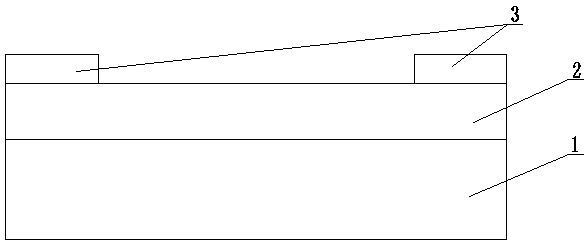
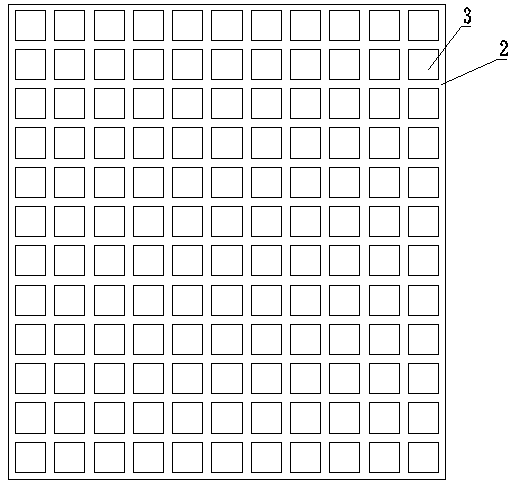
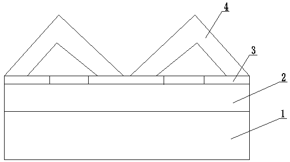
[0033] refer to Figure 1~3 , based on semipolar Al x Ga 1-x The specific process steps of the N material MSM ultraviolet detection device structure are as follows.

[0034] Step 1: First, ...


PUM


Abstract

The invention provides a production method of a high response ultraviolet detector, and belongs to the technical field of semiconductor device preparation. A mask layer with a strip-shaped or cross-shaped groove window is formed on a GaN seed crystal layer, and a growth mask is controlled to be arranged along a specified crystal orientation, then an MOCVD selective transverse epitaxy process is utilized to obtain a semi-polar crystal face AlxGa1-xN material with the low defect density, and finally a metal interdigital structure electrode is prepared on the surface of the AlxGa1-xN material toform a Schottky contact, so as to realize the high response ultraviolet detector.

Description

technical field [0001] The invention belongs to the technical field of semiconductor device preparation, and in particular relates to a processing technology of an ultraviolet detection device. Background technique [0002] Ultraviolet detection technology has extremely important applications in ultraviolet early warning and reconnaissance, ultraviolet communication, fire alarm system, environmental pollution monitoring, medical imaging and other fields. In recent years, GaN-based wide bandgap semiconductor materials (GaN, AlGaN) have gradually become the preferred material system for the preparation of ultraviolet detection devices. GaN-based semiconductor materials have high electron saturation velocity, high breakdown electric field, high thermal conductivity, high temperature resistance and The physical and chemical properties such as radiation resistance make the ultraviolet detection device work well under extreme conditions such as high temperature and spaceflight. A...

Claims


Application Information

Patent Timeline
Patent Type & Authority Applications(China)
IPC IPC(8): H01L31/108H01L31/0304H01L31/18
CPCY02P70/50
Inventor 徐峰陈鹏高峰汤文景张琳华雪梅
Owner 南京大学扬州光电研究院
Why Eureka
Try Eureka