Preparation method of film bulk acoustic resonator and filter
A thin-film bulk acoustic wave and resonator technology, which is applied in the field of microelectronics, can solve the problems of low power capacity, unsatisfactory compatibility, and high loss, and achieve the effects of high power tolerance, low loss, and high electromechanical coupling coefficient
- Summary
- Abstract
- Description
- Claims
- Application Information
AI Technical Summary
Problems solved by technology
Method used
Image
Examples
preparation example Construction
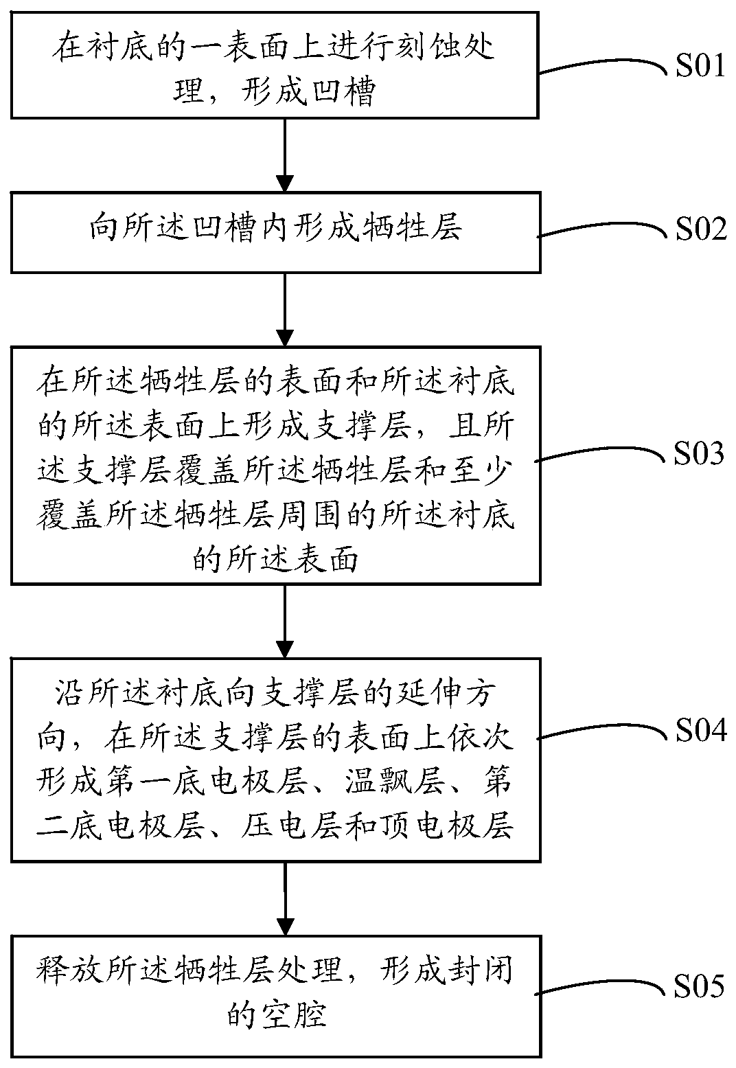
[0021] On the one hand, an embodiment of the present invention provides a method for preparing a thin film bulk acoustic resonator, combining figure 2 and image 3 , the process flow of the preparation method of the thin film bulk acoustic resonator is as follows figure 1 As shown, it includes the following steps:
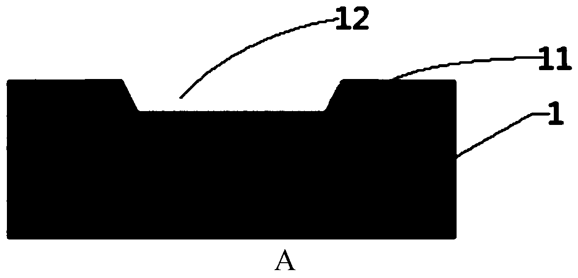
[0022] S01: Etching is performed on a surface 11 of the substrate 1 to form a groove 12, such as figure 2 As shown in A;
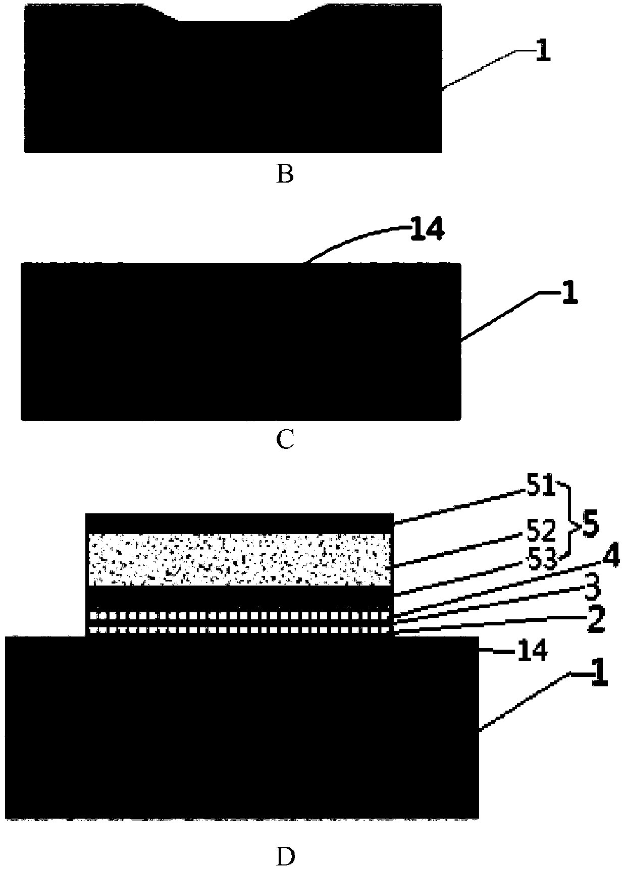
[0023] S02: Form a sacrificial layer 14 in the groove 12, such as figure 2 Shown in B and 2C;
[0024] S03: Form a supporting layer 2 on the surface of the sacrificial layer 14 and the surface 11 of the substrate 1, and the supporting layer 2 covers the sacrificial layer 14 and at least covers all surrounding areas of the sacrificial layer 14 The surface 11 of the substrate 1; as figure 2 as shown in D;
[0025] S04: Along the extending direction of the substrate 1 to the support layer 2, sequentially form the first bottom electrode ...
Embodiment 1
[0073] This embodiment provides a method for preparing a thin film bulk acoustic resonator. combine Figure 2-3 , the preparation method comprises the steps of:
[0074] Step S11: performing etching treatment on a surface 11 of the elemental silicon substrate 1 by dry etching to form a groove 12; wherein, the depth of the groove 12 is less than 3 μm, and the area of the groove 12 is preferably 1123 μm ×1123μm;
[0075] Step S12: growing amorphous SiO in the groove 12 and on the surface 11 by PECVD 2 layer (P on amorphous SiO 2 The percentage of atoms doped in can be controlled to 8%), and makes the grown amorphous SiO 2 The thickness of the layer exceeds the depth of the groove 12 and covers the surface 11 of the substrate 1; then chemical mechanical polishing (CMP) is used to treat the generated amorphous SiO with 100rpm 2 The layer is subjected to grinding treatment to remove the amorphous SiO grown on the surface 11 2 , so that the amorphous SiO filled in the groove...
Embodiment 2
[0081] This embodiment provides a method for preparing a thin film bulk acoustic resonator. combine Figure 2-3 , the preparation method comprises the steps of:
[0082] Step S11: performing etching treatment on a surface 11 of the elemental silicon substrate 1 by dry etching to form a groove 12; wherein, the depth of the groove 12 is less than 3 μm, and the area of the groove 12 is preferably 1123 μm ×1123μm;
[0083] Step S12: refer to step S12 in Embodiment 1;
[0084] Step S13: refer to step S13 in Embodiment 1;
[0085] Step S14: Follow step S14 in Example 1; wherein, the release reagent for releasing the sacrificial layer 14 includes HF and NH with a mass ratio of 1:3.8:2.3 3 F and glycerin.
[0086] The structure of the film bulk acoustic resonator formed by embodiment 2 is as follows image 3 As shown, the structure of the thin film bulk acoustic resonator is: substrate 1 / support layer 2 / first bottom electrode layer 3 / temperature floating layer 4 / second bottom ...
PUM
 Abstract
Description
Claims
Application Information


