A method, device and application of thinning silicon carbide sheet

A technology of silicon carbide wafers and silicon carbide, which is applied in the manufacture of electrical components, circuits, semiconductors/solid-state devices, etc., can solve the problem of unsuitable silicon carbide wafers, unsatisfactory thinning effects, silicon carbide wafers or silicon carbide wafers No problems such as thinning scheme

Active Publication Date: 2021-04-06
PEKING UNIV SHENZHEN GRADUATE SCHOOL
View PDF5 Cites 0 Cited by
  • Summary
  • Abstract
  • Description
  • Claims
  • Application Information

AI Technical Summary

Problems solved by technology

In the process of manufacturing silicon carbide semiconductors, especially in the latter part of the manufacturing process of silicon carbide power semiconductor products, the backside thinning back gold process will be carried out; however, there is currently no effective thinning method for silicon carbide wafers or silicon carbide wafers. Program
A similar thinning method is the thinning process of silicon wafers, but this solution is not suitable for silicon carbide wafers
Because the existing silicon wafer thinning process adopts a mechanical thinning method, that is, a silicon dioxide grinding head is used to grind and thin the silicon wafer; however, the hardness of the silicon dioxide grinding head is lower than that of the silicon carbide wafer. , so if you refer to the silicon wafer thinning method and perform mechanical thinning, not only can you not get a satisfactory thinning effect, but also the thinning grinding head of the silicon wafer will be scrapped, which greatly improves the production of silicon carbide wafer products cost
[0004] Therefore, there is currently no simple and effective thinning method for silicon carbide wafers, which is not conducive to the preparation and post-processing of silicon carbide wafers.

Method used


Image

  • A method, device and application of thinning silicon carbide sheet
  • A method, device and application of thinning silicon carbide sheet
  • A method, device and application of thinning silicon carbide sheet

Examples


Embodiment

[0059] The method for thinning silicon carbide wafers in this example includes pretreatment, deposition step, protective film removal step, thermal reaction step, film protection step, acid corrosion step, water washing step, mechanical grinding step and protective film removal step; Processing can be selected according to requirements. Each step is detailed as follows:

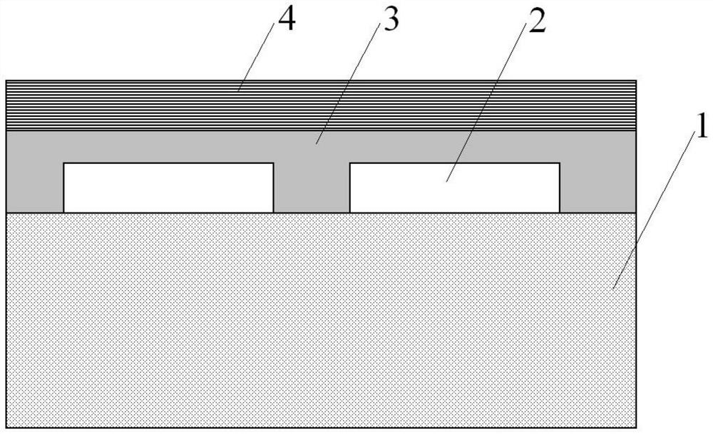
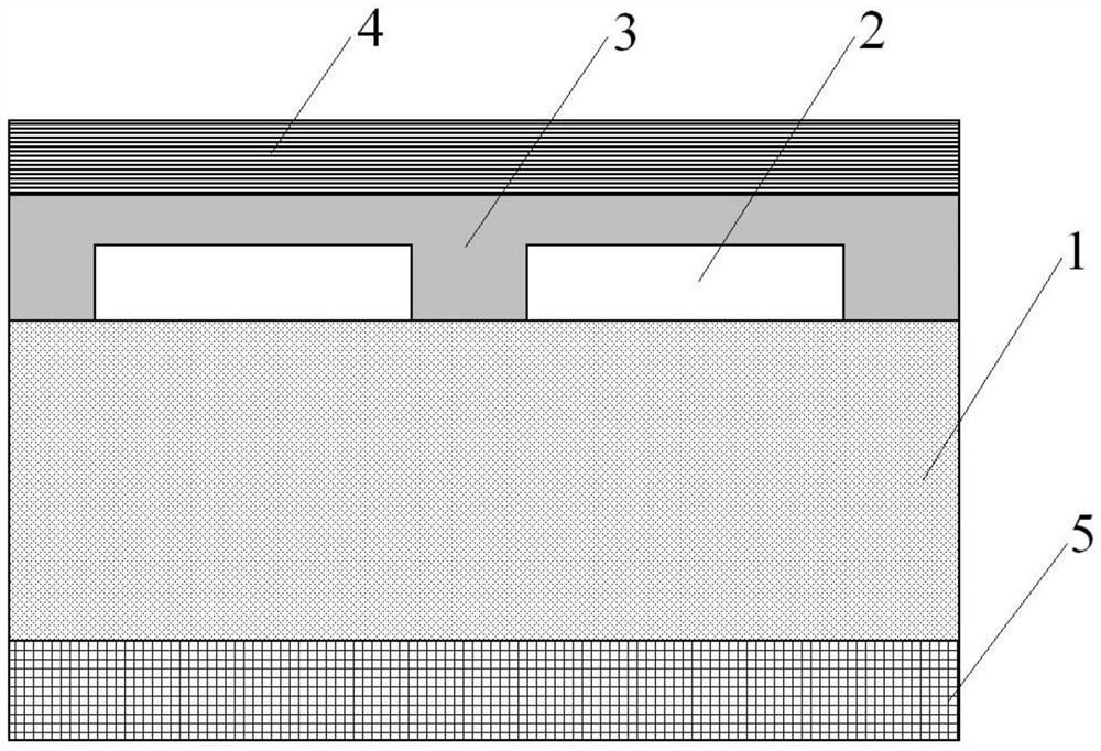
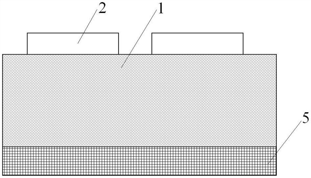
[0060] Pretreatment: After the normal silicon carbide wafer front-side device production process is completed, the front side of the silicon carbide wafer is coated with photoresist. Generally, the coating thickness of photoresist is 0.5-5μm, and then the front side is pasted with blue membrane protection, such as figure 1 as shown, figure 1 Among them, 1 is the silicon carbide wafer, 2 is the front device of the silicon carbide wafer, 3 is the photoresist, and 4 is the blue film; after pasting the blue film for protection, the silicon carbide wafer is soaked with 1% hydrofluoric acid After 0.5 to 10 minut...


PUM

PropertyMeasurementUnit
thicknessaaaaaaaaaa
thicknessaaaaaaaaaa
thicknessaaaaaaaaaa

Abstract

The application discloses a method, device and application for thinning a silicon carbide sheet. The method of the present application includes a deposition step of depositing a metal layer on the back of the silicon carbide wafer; a thermal reaction step of performing high-temperature heat treatment in an inert atmosphere; a film protection step of pasting a protective film on the front of the silicon carbide wafer; an acid etching step of using an acidic solution Soak the silicon carbide wafer; washing step, rinse the silicon carbide wafer with water and dry; mechanical grinding step, use the grinding head to grind the back of the silicon carbide wafer; remove the protective film step, remove the paste on the front of the silicon carbide wafer protective film. The method of the present application uses the metal in the metal layer to react with the silicon in the silicon carbide at high temperature to change the physical and chemical properties of the surface layer on the back of the silicon carbide, reduce the hardness of the surface layer, and make it possible to use silicon wafer thinning equipment normally. Thinning, not only has a good thinning effect, but also greatly reduces the production cost of silicon carbide wafer products.

Description

technical field [0001] The present application relates to the field of silicon carbide wafer preparation, in particular to a method, device and application for thinning silicon carbide wafers. Background technique [0002] As a new generation of wide bandgap semiconductor material, silicon carbide (SIC) has extremely excellent performance in the field of power semiconductors, and is the frontier and future direction of the development of power semiconductor devices. SiC (silicon carbide) is a compound semiconductor material composed of silicon (Si) and carbon (C), which has excellent electrical properties: for example, the forbidden band width is 2.3-3.3eV, which is 3 times that of Si; the breakdown field The strength is 0.8E16~3E16V / cm, which is 10 times that of Si; the saturation drift velocity is 2E7cm / s, which is 2.7 times that of Si; the thermal conductivity is 4.9W / cm K, which is about 3.2 times that of Si. These characteristics make silicon carbide materials have exc...

Claims


Application Information

Patent Timeline
Patent Type & Authority Patents(China)
IPC IPC(8): H01L21/04H01L21/67
CPCH01L21/0445H01L21/0475H01L21/67155
Inventor 林信南刘美华
Owner PEKING UNIV SHENZHEN GRADUATE SCHOOL
Why Eureka
Try Eureka