Lithium aluminate solid-state ion conduction layer, preparation method thereof, and all-solid-state electrochromic device comprising the same
An electrochromic device, ion conduction layer technology, applied in instruments, nonlinear optics, optics, etc., can solve the problems of slow response time, complexity and cost, poor stability, etc., to improve ion conductivity and ion conduction rate, The effect of avoiding ion loss and speeding up the response time
- Summary
- Abstract
- Description
- Claims
- Application Information
AI Technical Summary
Problems solved by technology
Method used
Image
Examples
Embodiment 1
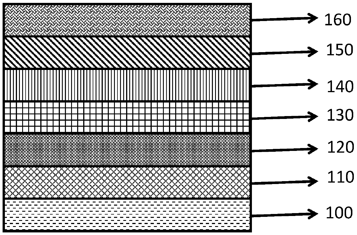
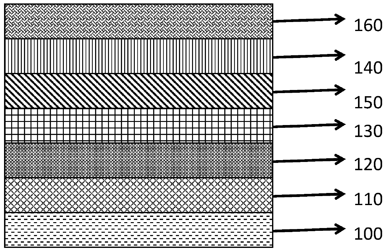
[0061] Clean the glass substrate, put it into the magnetron sputtering equipment, and sputter to form a transparent conductive material: the target material is ITO target material, the sputtering power supply is RF power supply, and the power density is 1w / cm 2 , the atmosphere is pure argon, the pressure is 0.5Pa, and the sputtering time is 60 minutes, an ITO conductive film with a smooth surface is obtained, and its thickness is 100-200nm. The surface resistance is measured, and the surface resistance is less than 50Ω.
Embodiment 2
[0063] Nickel oxide and zinc oxide mixed films are formed by sputtering on a glass substrate sputtered with transparent conductive materials: the target material is zinc-nickel target material, the sputtering power supply is DC power supply, and the power density is 1.5w / cm 2 , the atmosphere is pure argon, the pressure is 1.5Pa, and the sputtering time is 30 minutes, a nickel oxide zinc oxide mixed film with a smooth surface is obtained, and the thickness is 100-200nm. The surface resistance is measured, and the surface resistance is not less than 100kΩ.
Embodiment 3
[0065] Formation of lithium aluminate (LiAlO) on nickel oxide zinc oxide mixed film x ) Solid-state ion-conducting layer film: aluminum-lithium alloy Alx Li (x=1) is used as the target material, which is prepared by magnetron reactive sputtering method with DC power supply, and amorphous porous lithium aluminate (LiAlO x ) solid-state ion-conducting layer film, its thickness is 220nm, the specific preparation conditions are as follows: background vacuum 8 × 10 -4 Pa, the substrate temperature is 60°C, the sputtering working atmosphere is a mixed gas of oxygen and argon, in which the volume ratio of oxygen is 15%, the coating time is 50min, the working pressure is 2.5Pa, and the sputtering power density is 1.5W / cm 2 . Figure 4 Showing the resulting lithium aluminate (LiAlO x ) Transmission spectrum of the solid-state ion-conducting layer film. It can be seen that the visible light transmittance range of the solid ion conducting layer can reach more than 90%. Figure 5 Show...
PUM
| Property | Measurement | Unit |
|---|---|---|
| Surface resistance | aaaaa | aaaaa |
| Thickness | aaaaa | aaaaa |
| Thickness | aaaaa | aaaaa |
Abstract
Description
Claims
Application Information


