Super-junction power MOSFET (Metal-Oxide-Semiconductor Field Effect Transistor) with integrated resonant tunneling diode

A diode and integrated tunnel technology, applied in the field of superjunction power MOSFET, can solve the problems of increasing the specific on-resistance and leakage current of the device, reducing the stability of the device, etc., and achieve the effect of increasing the difficulty of the process and reducing the reverse recovery charge.

Active Publication Date: 2019-07-26
CHONGQING UNIV
View PDF6 Cites 5 Cited by
  • Summary
  • Abstract
  • Description
  • Claims
  • Application Information

AI Technical Summary

Problems solved by technology

However, while the above technology reduces the recovery charge in the body diode direction, it often redu

Method used


Image

  • Super-junction power MOSFET (Metal-Oxide-Semiconductor Field Effect Transistor) with integrated resonant tunneling diode
  • Super-junction power MOSFET (Metal-Oxide-Semiconductor Field Effect Transistor) with integrated resonant tunneling diode
  • Super-junction power MOSFET (Metal-Oxide-Semiconductor Field Effect Transistor) with integrated resonant tunneling diode

Examples


Embodiment 1

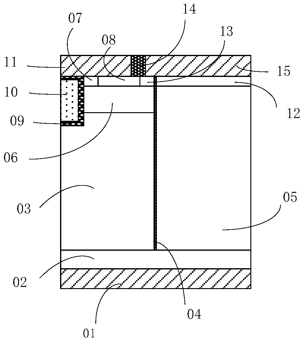
[0030] Example 1: figure 1 It is a super junction power MOSFET with integrated tunneling diode, which is composed of multiple repeating cell structures, including: drain terminal electrode 01, N-type substrate 02, N-type doped region 03, insulating layer I04 , P-type doped region I05, P-type doped region II06, N+ doped region I07, P+ doped region I08, gate oxide layer 09, polysilicon gate 10, source electrode 11, P+ doped region II12, N+ doped Region II13, insulating layer II14 and floating electrode 15;

[0031] The N-type substrate 02 is above the drain terminal electrode 01; the N-type doped region 03, the insulating layer I04, and the P-type doped region I05 are above the N-type substrate 02; the P-type doped region II06 is in the N-type doped Above region 03; N+ doped region I07, P+ doped region I08 and N+ doped region II13 are above P-type doped region II06;

[0032] The gate oxide layer 09 is surrounded by the N-type doped region 03, the P-type doped region II06 and t...

Embodiment 2

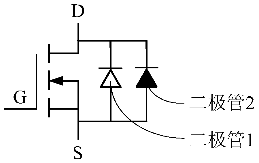
[0039] Embodiment 2: as Figure 5 As shown, the tunneling diode can also be constructed of polysilicon within the trench gate. The polysilicon gate 10 is N-type heavily doped in this embodiment, and a heavily doped P+ polysilicon I16 is introduced into the polysilicon gate 10 to form a tunneling diode. The floating electrode 15 is connected to the polysilicon gate 10 , and the P+ polysilicon is connected to the source electrode 11 .

Embodiment 3

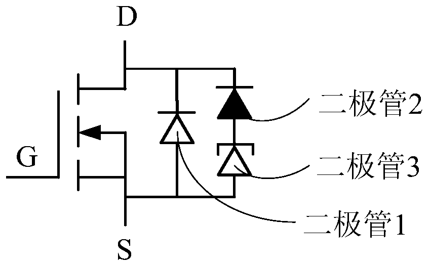
[0040] Embodiment 3: as Figure 6 As shown in Example 3, the polysilicon diode can also be formed of planar-gate polysilicon. The N+ polysilicon 19 and the P+ polysilicon II 20 together form a tunneling diode. The P+ doped region II12 is connected to the N+ polysilicon 19 through the floating electrode 15 , and the P+ polysilicon II20 is connected to the source electrode 11 .

[0041] In the above embodiments, the semiconductor material includes but not limited to silicon, germanium, gallium arsenide, silicon carbide or gallium nitride; the insulating layer material includes but not limited to silicon dioxide, silicon nitride or barium strontium titanate.


PUM


Abstract

The invention relates to a super-junction power MOSFET (Metal-Oxide-Semiconductor Field Effect Transistor) with an integrated resonant tunneling diode, and belongs to the field of semiconductor powerdevices. The MOSFET comprises a drain end electrode, an N type substrate, an N type doping area, an insulating layer I, a P type doping area I, a P type doping area II, an N+ doping area I, a P+ doping area I, a gate oxide layer, a polysilicon gate, a source end electrode, a P+ doping area II, an N+ doping area II, an insulating layer II and a floating electrode. Through adoption of the super-junction power MOSFET, the reverse recovery charge of a device can be reduced greatly under the condition of not increasing the specific on-resistance and drain current of the device, and the technological difficulty is not increased.

Description

technical field [0001] The invention belongs to the field of semiconductor power devices and relates to a super junction power MOSFET with an integrated tunneling diode. Background technique [0002] Superjunction MOSFET (SuperJunction Metal-Oxide-Semiconductor Field Effect Transistor), that is, metal-oxide-semiconductor field effect transistor, can improve the contradiction between breakdown voltage and specific on-resistance in traditional power MOSFET devices, and has extremely low specific conduction Resistance and extremely fast switching speed are widely used in industry, new energy, information transportation and other fields. However, the body diode of the super-junction MOSFET has a large reverse recovery charge, which will reduce the efficiency of the power converter using the super-junction MOSFET and increase the noise of the power converter. [0003] In order to reduce the reverse recovery charge of the body diode, carrier lifetime control technology is usually...

Claims


Application Information

Patent Timeline
IPC IPC(8): H01L29/78
CPCH01L29/7803H01L29/7813
Inventor 李平郭经纬林智胡盛东唐枋
Owner CHONGQING UNIV
Why Eureka
Try Eureka