Three-dimensional optoelectronic integrated optical grating coupler realized based on CMOS post-process and preparation method thereof

A grating coupler and optoelectronic integration technology, applied in the direction of optical waveguide light guide, light guide, optics, etc., can solve the problem of increasing optical coupling loss and achieve the effect of increasing bandwidth

Active Publication Date: 2019-07-30
INST OF SEMICONDUCTORS - CHINESE ACAD OF SCI
View PDF8 Cites 0 Cited by
  • Summary
  • Abstract
  • Description
  • Claims
  • Application Information

AI Technical Summary

Problems solved by technology

If the spacing of different planar optoelectronic device layers deviates from the i

Method used


Image

  • Three-dimensional optoelectronic integrated optical grating coupler realized based on CMOS post-process and preparation method thereof
  • Three-dimensional optoelectronic integrated optical grating coupler realized based on CMOS post-process and preparation method thereof
  • Three-dimensional optoelectronic integrated optical grating coupler realized based on CMOS post-process and preparation method thereof

Examples


Example Embodiment

[0040] In order to make the objectives, technical solutions and advantages of the present invention clearer, the present invention will be further described in detail below in conjunction with specific embodiments and with reference to the accompanying drawings.

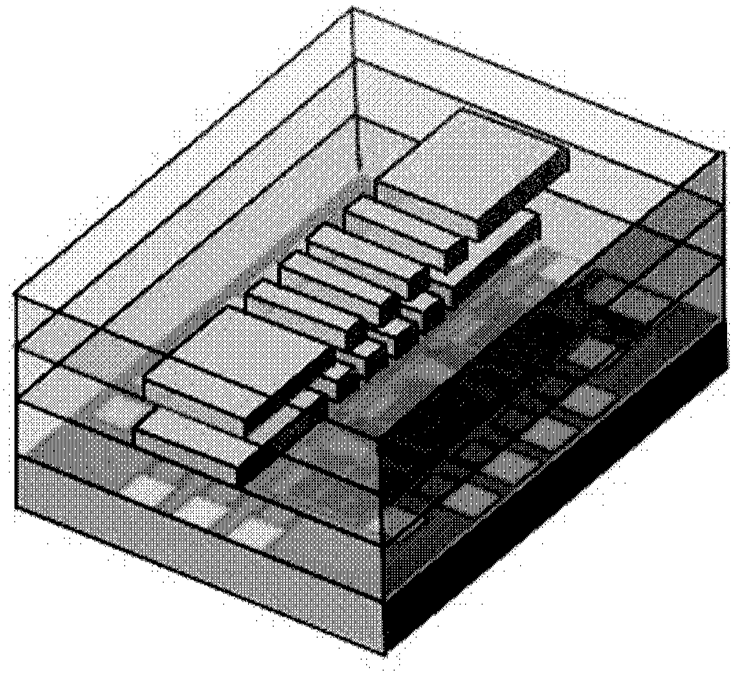
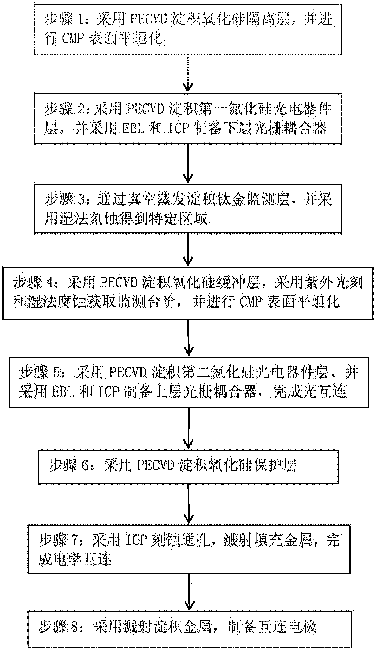
[0041] The present invention proposes a three-dimensional photoelectric integrated grating coupler realized based on CMOS post-process. All process temperatures are controlled below 400°C to avoid impact on CMOS integrated circuits, realize monolithic integration of photoelectric devices and CMOS integrated circuits, and realize three-dimensional Optical interconnection solves the bottleneck problem of electrical interconnection.

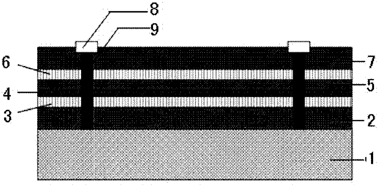
[0042] Reference figure 1 with figure 2 The three-dimensional photoelectric integrated grating coupler realized by the present invention based on the CMOS post process includes a silicon oxide isolation layer 2, a first silicon nitride photoelectric device layer 3, and a titanium-gold monitorin...


PUM

PropertyMeasurementUnit
Thicknessaaaaaaaaaa
Thicknessaaaaaaaaaa
Thicknessaaaaaaaaaa

Abstract

The invention relates to a three-dimensional optoelectronic integrated optical grating coupler and a preparation method thereof. The three-dimensional optoelectronic integrated optical grating couplercomprises an isolation layer, a first optoelectronic device layer, a monitoring layer, a buffer layer, a second optoelectronic device layer and a protection layer which are deposited on a CMOS integrated circuit from bottom to top, wherein a plurality of through holes penetrate through all the layers, the through holes are filled with metal which is in contact with electrodes of the CMOS integrated circuit, and interconnection electrodes are arranged above the through holes; the first optoelectronic device layer is used for preparing a lower-layer optical grating coupler which interacts withthe CMOS integrated circuit; the second optoelectronic device layer is used for preparing an upper-layer optical grating coupler which is in optical interconnection with the first optoelectronic device layer. The single-chip integration of the optical grating coupler and the CMOS integrated circuit can be realized, three-dimensional optical interconnection is realized, the transmission loss of inter-layer optical interconnection is reduced, and the inter-layer coupling efficiency is maximized. The coupler is compatible with a CMOS technology, is easy to prepare, can be used for three-dimensional optoelectronic integration, and realizes integration of a high-density optoelectronic device and a microelectronic circuit.

Description

Technical field [0001] The invention relates to the technical field of photoelectric integration, in particular to a three-dimensional photoelectric integrated grating coupler realized based on a CMOS post process and a preparation method thereof. Background technique [0002] With the continuous development of integrated circuit technology in the direction of high speed and high integration, Moore's Law is facing the ultimate challenge of chip integration. Traditional electrical interconnection inevitably has problems such as high delay, high power consumption and serious signal crosstalk. So people turned their attention to a new generation of interconnection technology-optical interconnection. Optical interconnection has the advantages of wide bandwidth, anti-electromagnetic interference, strong confidentiality, low loss and low power consumption, while silicon-based optical interconnection can play the advantages of wide bandwidth, low crosstalk, low loss and compatibility wi...

Claims


Application Information

Patent Timeline
IPC IPC(8): G02B6/124G02B6/12
CPCG02B6/12002G02B6/124G02B2006/12147G02B2006/12166
Inventor 黄北举张欢程传同陈弘达
Owner INST OF SEMICONDUCTORS - CHINESE ACAD OF SCI
Why Eureka
Try Eureka