Light emitting device, preparation method thereof and application

A light-emitting device and a common technology, which is applied in the manufacture of semiconductor/solid-state devices, electric solid-state devices, semiconductor devices, etc., can solve the problems of increasing the luminous efficiency of light-emitting devices, the inability to produce green effects, and the luminous efficiency to be improved, so as to improve the appearance Effects of quantum efficiency, improved recombination efficiency, and low cost

Pending Publication Date: 2019-08-02
SHENZHEN PLANCK INNOVATION TECH CO LTD
View PDF3 Cites 3 Cited by
  • Summary
  • Abstract
  • Description
  • Claims
  • Application Information

AI Technical Summary

Problems solved by technology

However, it is only a quantum dot with a core-shell structure, not a quantum rod structure, and cannot produce a green effect
[0005] CN106410058A discloses a method for making a quantum dot light-emitting device, which includes: providing a substrate, and making an anode on the substrate by sputtering deposition; making hole injection on the anode by suspension coating, atomization or inkjet printing process layer; by suspension coating, inkjet printing or atomization process, the hole transport layer is coated on the hole injection layer; by suspension coating, inkjet printing or atomization process, the quantum dot light-emitting layer is coated on the hole transport layer; by sputtering deposition or solution method, the IZO electron transport layer is deposited on the quantum dot light-emitting layer; and by thermal evaporation process, the cathode is made on the IZO electron transport layer to obtain the corresponding quantum dot light-emitting device; the method Preparation improves the luminous efficiency of quantum dot light-emitting devices, but its luminous efficiency still needs to be improved
The quantum dot light-emitting device includes: a first electrode and a second electrode; a quantum dot light-emitting layer located between the first electrode and the second electrode; a quantum dot light-emitting layer located between the first electrode The first hole transport layer; the hole injection layer between the first hole transport layer and the first electrode; the electron transport layer between the quantum dot light emitting layer and the second electrode and a filling layer located between the electron transport layer and the quantum dot light-emitting layer and embedded in the quantum dot light-emitting layer; the quantum dot light-emitting device provided by the invention can effectively prevent leakage, thereby reducing the current density, However, there is no mention of the ability to increase the luminous efficiency of light-emitting devices

Method used


Image

  • Light emitting device, preparation method thereof and application
  • Light emitting device, preparation method thereof and application
  • Light emitting device, preparation method thereof and application

Examples


Embodiment 1

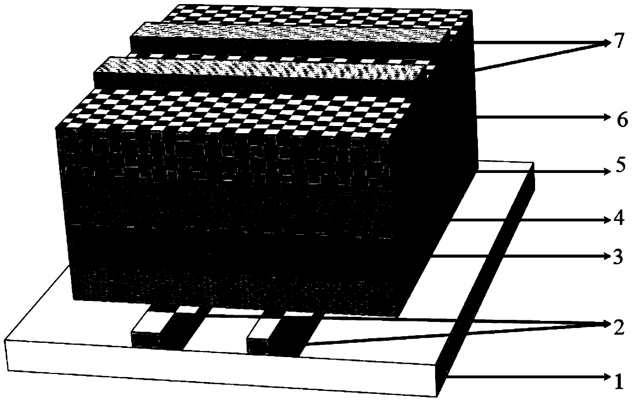
[0114] This embodiment provides a light emitting device, such as figure 1 As shown: the light-emitting device sequentially includes a base layer 1, an anode layer 2, a first hole transport layer 3, a second hole transport layer 4, a quantum rod layer 5, and an electron transport layer 6 combined together from bottom to top And cathode layer 7, wherein base layer 1 is a glass base layer; Anode layer 2 is an ITO conductive glass layer; The first hole transport layer 3 is a PEDOT:PSS hole transport layer; The second hole transport layer 4 is a PVK hole Transport layer; the quantum rod layer 5 is a CdSe / CdS quantum rod layer in the red light band, and its fluorescence emission wavelength is 630nm; the electron transport layer 6 is a ZnMgO layer; the cathode layer 7 is an aluminum electrode layer, and its thickness is 500nm.

[0115] This embodiment also provides a method for preparing a light-emitting device, and the method includes the following steps:

[0116] (1) Deposit an IT...

Embodiment 2

[0124] This embodiment provides a light-emitting device, the light-emitting device sequentially includes a base layer, an anode layer, a first hole transport layer, a second hole transport layer, a quantum rod layer, and an electron transport layer combined together from bottom to top. And the cathode layer, wherein the base layer is a glass base layer; the anode layer is an ITO conductive glass layer; the first hole transport layer is a PEDOT:PSS hole transport layer; the second hole transport layer is a PVK hole transport layer; The layer is a CdSe / CdS quantum rod layer in the red light band, and its fluorescence emission wavelength is 600nm; the electron transport layer is a ZnMgO layer; the cathode layer is an aluminum electrode layer, and its thickness is 1000nm.

[0125] This embodiment also provides a method for preparing a light-emitting device, and the method includes the following steps:

[0126] (1) Deposit an ITO conductive film on the glass base layer, obtain the ...

Embodiment 3

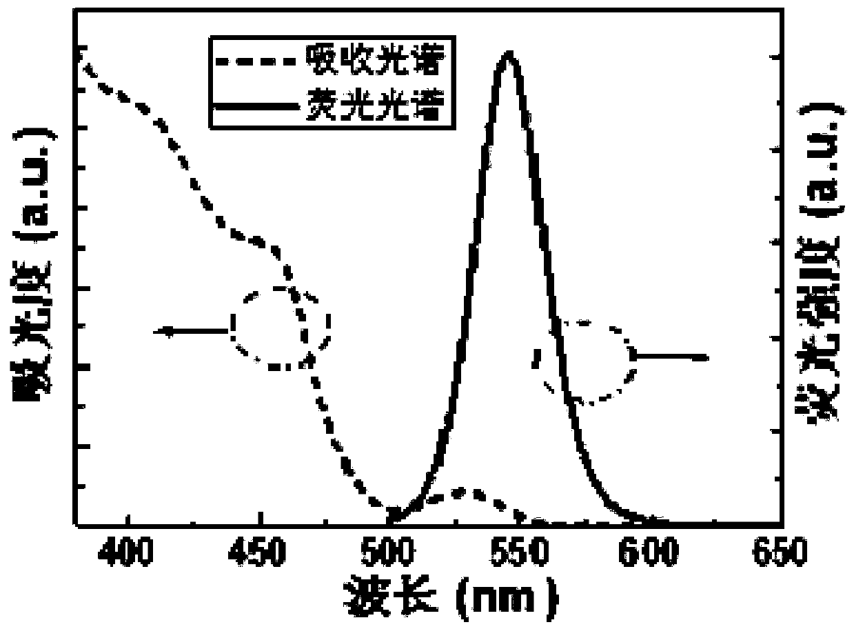
[0134]This embodiment provides a light-emitting device, the light-emitting device sequentially includes a base layer, an anode layer, a first hole transport layer, a second hole transport layer, a quantum rod layer, and an electron transport layer combined together from bottom to top. And the cathode layer, wherein the base layer is a glass base layer; the anode layer is an ITO conductive glass layer; the first hole transport layer is a PEDOT:PSS hole transport layer; the second hole transport layer is a PVK hole transport layer; The layer is a CdSe / CdS quantum rod layer in the green light band, and its fluorescence emission wavelength is 560nm; the electron transport layer is a ZnMgO layer; the cathode layer is an aluminum electrode layer, and its thickness is 100nm.

[0135] This embodiment also provides a method for preparing a light-emitting device, and the method includes the following steps:

[0136] (1) Deposit an ITO conductive film on the glass base layer, obtain the ...


PUM


Abstract

The invention provides a light emitting device. The light emitting device comprises a base layer, an anode layer, a first hole transport layer, a second hole transport layer, a quantum rod layer, an electron transport layer and a cathode layer which are combined together sequentially from bottom to top. Through replacing a quantum dot light emitting layer in the conventional application as the quantum rod light emitting layer, the external quantum efficiency of the light emitting device can be improved; the quantum rod light emitting layer is a quantum rod layer with a fluorescence wavelengthof 500 to 700 nm, self absorption of the light emitting device can be further reduced, and the external quantum efficiency can be further increased; through using a specific ligand octadecylphosphonicacid to prepare a CdSe core quantum dot and coating the CdSe core quantum dot, fluorescence red shift to a green band, the effect of generating green can be achieved, and the external quantum efficiency of a green light emitting device can be further improved; and the light emitting device preparation method is simple, the raw material is easy to obtain, realization is easy, and wide applicationto industrial production is facilitated.

Description

technical field [0001] The invention belongs to the field of light-emitting devices, and relates to a light-emitting device and a preparation method and application thereof. Background technique [0002] Compared with the traditional liquid crystal display technology, the new quantum dot electroluminescent diode device has the advantages of wide color gamut, high efficiency, and the ability to produce flexible displays. It is very likely to replace the traditional liquid crystal display technology and become a new generation of widely used display technology . As a deformed semiconductor nanocrystal of quantum dots, quantum rods not only have all the advantages of quantum dots, but also have unique characteristics such as ultra-low self-absorption and polarized luminescence. Therefore, replacing quantum dots with quantum rods to make electroluminescent diode devices can further improve the efficiency and function of display devices. [0003] However, at present, the work o...

Claims


Application Information

Patent Timeline
Patent Type & Authority Applications(China)
IPC IPC(8): H01L51/50H01L51/54H01L51/56B82Y40/00
CPCB82Y40/00H10K50/115H10K2102/00H10K71/00
Inventor 孙小卫王恺周子明徐冰
Owner SHENZHEN PLANCK INNOVATION TECH CO LTD
Why Eureka
Try Eureka