Low-pressure preparation method for silicon carbide thin film epitaxy

A silicon carbide and silicon carbide substrate technology, applied in chemical instruments and methods, gaseous chemical plating, from chemically reactive gases, etc., can solve the problems of epitaxial surface morphology degradation, material quality reduction, etc., to reduce surface defects Density, avoidance of deposits, effect of improving quality

Inactive Publication Date: 2019-08-13
XIDIAN UNIV
View PDF8 Cites 3 Cited by
  • Summary
  • Abstract
  • Description
  • Claims
  • Application Information

AI Technical Summary

Problems solved by technology

Si droplets can be deposited on the substrate, leading to degradation of the epitaxial surface topography and reduction of material quality

Method used


Image

  • Low-pressure preparation method for silicon carbide thin film epitaxy

Examples


Embodiment 1

[0025] see figure 1 , figure 1 A schematic structural diagram of a virtual LED display module based on a three-color I-shaped LED chip provided by an embodiment of the present invention.

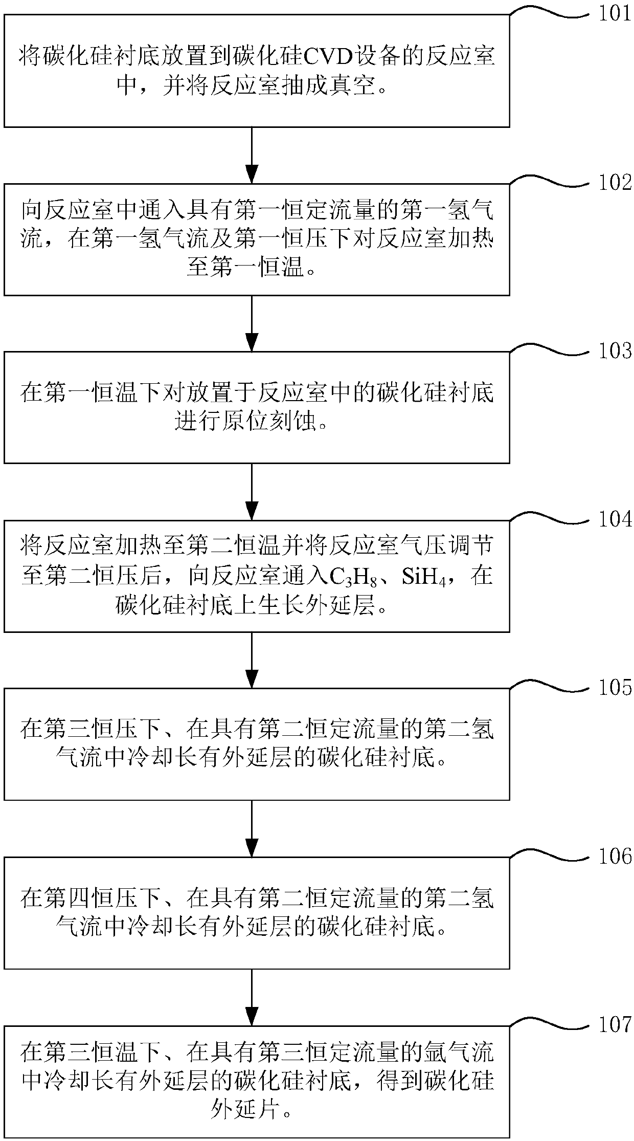
[0026] 101. Put the silicon carbide substrate into the reaction chamber of the silicon carbide CVD equipment, and evacuate the reaction chamber. CVD stands for Chemical Vapor Deposition. This step specifically includes:

[0027] 101a. Selecting a silicon carbide substrate;

[0028] In one embodiment of the present invention, a 4H silicon carbide substrate with a 4° orientation to [1120] is selected;

[0029] In another embodiment of the present invention, a 4H silicon carbide substrate with an orientation of 8° to [1120] is selected;

[0030] 101b. Evacuate the reaction chamber, specifically to make the pressure of the reaction chamber lower than 1×10 -7 mbar.

[0031] 102. Introduce a first hydrogen flow with a first constant flow rate into the reaction chamber, and heat the reaction...


PUM


Abstract

The invention relates to a low-pressure preparation method for a silicon carbide thin film epitaxy. The method comprises the steps that a silicon carbide substrate is placed in a reaction chamber of silicon carbide CVD equipment, and the reaction chamber is vacuumized; first hydrogen flow with a first constant flow rate is introduced into the reaction chamber, and under the first hydrogen flow andthe first constant pressure, the reaction chamber is heated to a first constant temperature; at the first constant temperature, the silicon carbide substrate placed in the reaction chamber is subjected to in-situ etching; after the reaction chamber is heated to a second constant temperature, the air pressure of the reaction chamber is adjusted to the second constant pressure, C3H8 and SiH4 are introduced into the reaction chamber, and an epitaxial layer grows on the silicon carbide substrate; under the third constant pressure, the silicon carbide substrate with the epitaxy layer growing on iscooled in second hydrogen flow with a second constant flow rate; under the fourth constant pressure, the silicon carbide substrate with the epitaxy layer growing on is cooled in the second hydrogen flow; at a third constant temperature, the silicon carbide substrate with the epitaxy layer growing on is cooled in argon flow with a third constant flow rate, and a silicon carbide epitaxy wafer is obtained.

Description

technical field [0001] The invention relates to the technical field of semiconductor device manufacturing, in particular to a method for preparing silicon carbide thin film epitaxy under low pressure. Background technique [0002] Silicon carbide has the advantages of wide band gap, high thermal conductivity, high breakdown strength, high electron saturation drift velocity, high hardness, etc., and also has strong chemical stability. These excellent physical and electrical properties make silicon carbide have many advantages in application. The forbidden band allows silicon carbide intrinsic carriers to maintain a low concentration at high temperatures, so it can work at very high temperatures. The high breakdown field strength enables silicon carbide to withstand high electric field strength, which allows silicon carbide to be used to make high-voltage, high-power semiconductor devices. The high thermal conductivity makes silicon carbide have good heat dissipation, which ...

Claims


Application Information

Patent Timeline
Patent Type & Authority Applications(China)
IPC IPC(8): C30B29/36C30B25/02C23C16/32C23C16/44
CPCC23C16/325C23C16/44C30B25/02C30B29/36
Inventor 韩超胡继超张玉明贾仁需郭辉王雨田
Owner XIDIAN UNIV
Why Eureka
Try Eureka