LDMOS device resistant to total dose effect

An anti-total dose and effect technology, applied in semiconductor devices, electrical components, circuits, etc., can solve the problems of reducing gate oxygen high voltage tolerance, affecting device performance, device performance parameter degradation and failure, etc., to improve the total dose reinforcement ability. , the effect of suppressing threshold voltage drift and leakage

Inactive Publication Date: 2019-08-16
UNIV OF ELECTRONICS SCI & TECH OF CHINA
View PDF10 Cites 11 Cited by
  • Summary
  • Abstract
  • Description
  • Claims
  • Application Information

AI Technical Summary

Problems solved by technology

figure 1 The LDMOS device shown uses RESURF (Reduced SURface Field) technology and field plate technology to improve the withstand voltage capability. When the device works in a radiation environment, its very thick high-voltage insulating oxide layer will continuously accumulate oxide trap charges and The interface state charge makes the performance parameters of the device gradually degrade and fail, such as the decrease of the electron mobility of the inversion layer, the increase of the leakage current and the drift of the threshold voltage, etc., causing the device to not be turned on and off normally, and resulting in an increase in the overall power consumption of the circuit
[0004] In order to suppress the failure of the total dose of the device, a common method is to thin the thickness of the gate oxide, but this also reduces the high-voltage withstand capability o...

Method used


Image

  • LDMOS device resistant to total dose effect
  • LDMOS device resistant to total dose effect
  • LDMOS device resistant to total dose effect

Examples


Embodiment Construction

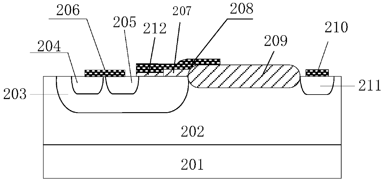
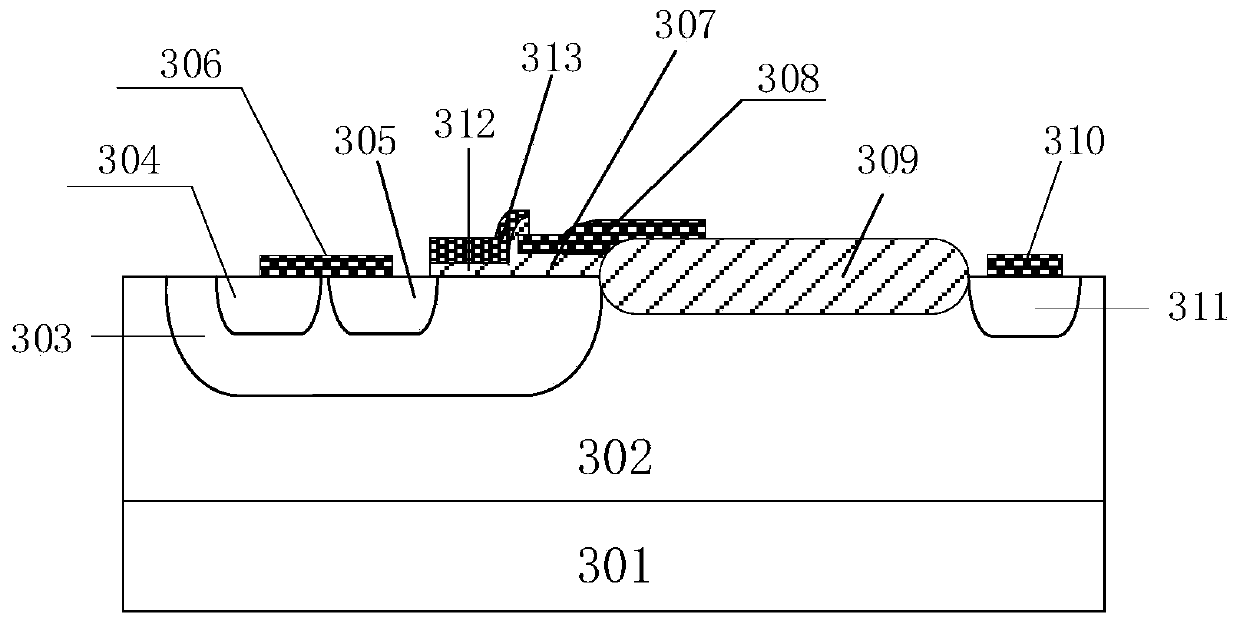
[0027] The present invention proposes a LDMOS device structure with total dose effect hardening capability, and its specific structure is as follows figure 2 with image 3 shown. figure 2 The device shown has a thin gate oxide (212) and a thick gate oxide (207). The amount of transistor threshold voltage shift induced by total dose radiation is generally proportional to the square of the thickness of the gate oxide, so the thinner gate oxide The threshold voltage shift caused by the total dose effect is relatively small. image 3 The device can be regarded as a double gate oxide device including a thin oxide layer gate (313) and a thick oxide layer gate (308). Applying an appropriate voltage to the two gates can turn on the device, but when any one of the devices is turned on alone The LDMOS is not turned on.

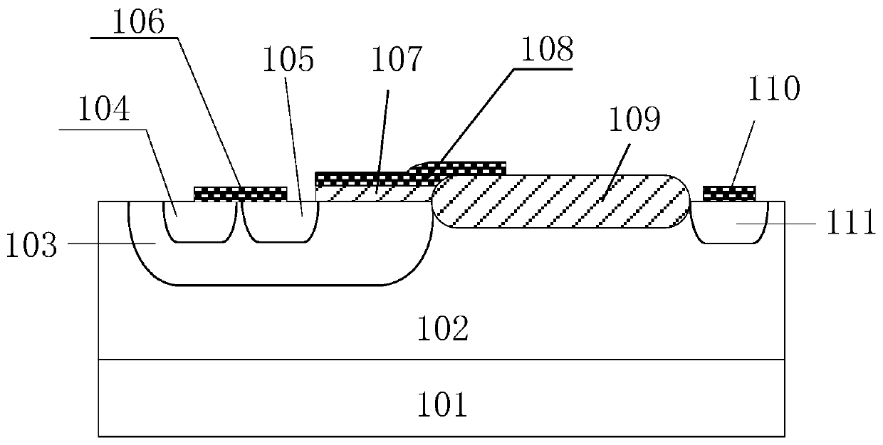
[0028] when figure 1 When the device shown is subjected to total dose effect radiation, the thickness of its gate oxide layer (107) is much greater than that of a...


PUM


Abstract

The invention belongs to the technical field of radiation-resistant semiconductors. The invention provides a novel LDMOS power device structure which can greatly enhance the total dose effect reinforcement capability of an LDMOS device. LDMOS devices are often used in high-voltage high-power fields. For an LDMOS device withstanding a working voltage of 20V, the thickness of the high-voltage-resistant gate oxide layer is usually dozens of micrometers. The invention, in view of the total dose effect sensitivity of a thick gate oxide layer, provides a method for introducing a thin gate oxide structure into a region close to the source of the thick gate oxide layer in order to form a novel LDMOS device having double gate oxide layers. The novel LDMOS device has beneficial effects that the newly introduced thin gate oxide region still turns off the entire LDMOS device when the high-voltage-resistant thick gate oxide region is affected by a serious space radiation total dose effect; due to the case that the anti-total dose effect capability of the thin oxide layer is better than that of the thick gate oxide, the leakage current between the source and the drain can be suppressed, so thatthe LDMOS device can obtain a good total dose reinforcement effect; and the structure cannot causes other problems such as an increase in area and process incompatibility.

Description

technical field [0001] The present invention relates to integrated circuits, and more particularly to LDMOS devices. Background technique [0002] Semiconductor power devices are another technological highland in the semiconductor industry besides the three major industries of application-specific integrated circuits, semiconductor equipment, and integrated circuit design simulation and design software. Laterally Diffused MOSFET (LDMOS) power devices have the characteristics of high operating voltage and good process compatibility, and are widely used in power switching conversion, microwave / RF power amplification, high-voltage output and other fields. [0003] Such as figure 1 The cross-sectional view of a conventional LDMOS device shown includes 101P-substrate, 102N-drift region, 103P well, 104P+ region, 105N+ source region, 106 source, 107 gate oxide layer, 108 gate, 109 field oxygen, 110 drain , 111N+ drain region. figure 1 The LDMOS device shown uses RESURF (Reduced ...

Claims


Application Information

Patent Timeline
IPC IPC(8): H01L29/423H01L29/78
CPCH01L29/42364H01L29/7816
Inventor 廖永波徐博洋李平黄德刘承鹏刘涛
Owner UNIV OF ELECTRONICS SCI & TECH OF CHINA
Why Eureka
Try Eureka