Eureka AIR delivers breakthrough ideas for toughest innovation challenges, trusted by R&D personnel around the world.

Lossless buffer circuit for suppressing GaN half-bridge module voltage spike and current resonance and test circuit thereof

A buffer circuit, voltage spike technology, applied in electronic circuit testing, high-efficiency power electronic conversion, measurement of electricity and other directions, can solve problems such as endangering system stability, fast switching speed, etc., to avoid current oscillation, suppress voltage spikes and current resonance, The effect of promoting the stability of the system

Active Publication Date: 2019-08-16
HARBIN INST OF TECH
View PDF6 Cites 9 Cited by
  • Summary
  • Abstract
  • Description
  • Claims
  • Application Information

AI Technical Summary

Problems solved by technology

[0005] For the existing half-bridge modules using GaN power devices, the voltage and current spikes caused by the fast switching speed of the power devices will endanger the stability of the system. The present invention provides a non-destructive buffer that suppresses the voltage spikes and current resonance of GaN half-bridge modules. Circuit and its test circuit

Method used


Image

  • Lossless buffer circuit for suppressing GaN half-bridge module voltage spike and current resonance and test circuit thereof
  • Lossless buffer circuit for suppressing GaN half-bridge module voltage spike and current resonance and test circuit thereof
  • Lossless buffer circuit for suppressing GaN half-bridge module voltage spike and current resonance and test circuit thereof

Examples


specific Embodiment approach 1

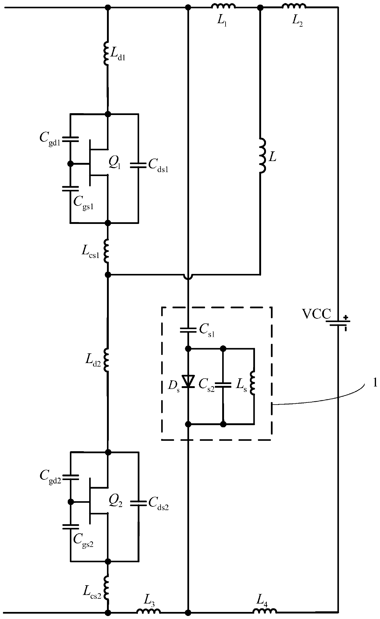
[0029] Specific implementation mode 1. Combination figure 1 As shown, the first aspect of the present invention provides a non-destructive snubber circuit that suppresses voltage spikes and current resonance of a GaN half-bridge module. Composed in series; the lossless snubber circuit is connected between the drain of the power device of the upper bridge arm and the source of the power device of the lower bridge arm of the GaN half-bridge module.

[0030] The non-destructive snubber circuit described in this embodiment is used in a GaN half-bridge module, which can alleviate the large turn-off voltage peak and the resonant current in the power loop caused by the fast switching process of the power device. The specific connection relationship between it and the GaN half-bridge module is as follows: figure 1 shown in .

[0031] As an example, combining figure 1 As shown, the lossless snubber circuit can adopt the following specific connection relationship: including the induc...

specific Embodiment approach 2

[0049] Specific embodiment two, combine figure 1 As shown, another aspect of the present invention also provides a test circuit for a non-destructive snubber circuit, the non-destructive snubber circuit comprising the suppressing GaN half-bridge module voltage spike and A non-destructive snubber circuit for current resonance, the test circuit includes the upper bridge arm power device Q of the GaN half bridge module 1 , Lower arm power device Q 2 , lossless snubber circuit, load inductance L, DC source VCC, power loop parasitic inductance L 1 , Power loop parasitic inductance L 2 , Power loop parasitic inductance L 3 , Power loop parasitic inductance L 4 ;

[0050] For the high-side power device Q 1 , whose gate-to-drain parasitic capacitance is C gd1 , the gate-to-source parasitic capacitance is C gs1 , the drain-source parasitic capacitance is C ds1 , the drain parasitic inductance is L d1 , the source parasitic inductance is L cs1 ;

[0051] For the lower bridge...

specific Embodiment

[0060] Specific embodiments: Taking the GaN HEMT semiconductor device GS66508B of GaN Systems Company as an example, the bus voltage of the test circuit is designed to be 400V, and the peak voltage is allowed to be 450V. According to the above calculation method, the absorbing capacitance C s1 The value is 100nF, C s2 The value is 10nF, L s The value is 0.3uH. It has been tested and verified that the non-destructive snubber circuit that suppresses the resonance of the turn-off peak voltage and current does not increase the snubber loss, and can simultaneously suppress the resonance of the peak voltage and the module outlet current.

[0061] In order to compare the effect of the present invention on suppressing voltage spikes and current resonance, this embodiment is based on the Pspice simulation model of the GS66508B chip, and a Pspice-based double-pulse test simulation platform can be built, and compared with no buffer circuit and single capacitor buffer circuit. The above ...


PUM


Abstract

The invention provides a lossless buffer circuit for suppressing GaN half-bridge module voltage spike and current resonance and a test circuit thereof, belongs to the technical field of wide band gapsemiconductor power device driving, and aims at the problem that the voltage and current spike caused by the high switching speed of the power device endangers the stability of the system in the existing half-bridge module using the GaN power device. The lossless buffer circuit is mainly composed in a way that an inductor, a capacitor and a diode are connected in parallel in turn and then connected in series with another capacitor. The lossless buffer circuit is connected between the upper bridge arm power device drain and the lower bridge arm power device source of the GaN half-bridge module.When the parasitic inductance current of the power loop of the bridge circuit topology changes, a low impedance loop can be provided so as to suppress the spike voltage of the two ends of the power device and destroy the current resonance loop in the GaN half-bridge module and thus the current oscillation at the module outlet can be avoided.

Description

technical field [0001] The invention belongs to the technical field of driving wide bandgap semiconductor power devices, in particular to a non-destructive snubber circuit and a test circuit for suppressing voltage spikes and current resonance of a GaN half-bridge module. Background technique [0002] Gallium nitride (GaN) semiconductor power devices and silicon carbide semiconductor power devices belong to the third-generation semiconductor power devices. Compared with silicon-based semiconductor devices, they have the advantages of fast switching speed, high operating frequency, and small switching loss and conduction loss. . In addition, GaN power devices have no parasitic body diode and no reverse recovery loss compared with MOSFETs, so they are more suitable for bridge topology applications. With the development, the power level of GaN power devices has been greatly improved at present. Commercial GaN power devices with a withstand voltage level of 600V have entered th...

Claims


Application Information

Patent Timeline
Patent Type & Authority Applications(China)
IPC IPC(8): H02M1/34G01R31/28
CPCG01R31/282H02M1/34H02M1/346Y02B70/10
Inventor 王高林李斌兴刘少博张容驰赵楠楠霍军亚朱良红徐殿国
Owner HARBIN INST OF TECH
Why Eureka
Eureka Blog
Learn More