Supercharge Your Innovation With Domain-Expert AI Agents!

An anode-short-circuit lateral insulated gate bipolar transistor eliminating negative resistance effect

A technology of bipolar transistors and field effect transistors, applied in circuits, semiconductor devices, electrical components, etc., can solve the problems of increasing device conduction loss, large conduction voltage drop, device failure, etc., and achieve the goal of eliminating negative resistance effect Effect

Active Publication Date: 2022-03-08
SOUTHEAST UNIV
View PDF0 Cites 0 Cited by
  • Summary
  • Abstract
  • Description
  • Claims
  • Application Information

AI Technical Summary

Problems solved by technology

However, these devices will bring some new problems while increasing the turn-off speed. Due to the existence of N-type heavily doped regions in the anode region, there are two different conductive forms of unipolar and bipolar when the device is turned on. , resulting in a serious negative resistance phenomenon
The negative resistance effect will cause the device to have a large conduction voltage drop when it is just turned on, which greatly increases the conduction loss of the device and reduces the conduction performance of the device; not only that, but the large voltage change caused by the negative resistance effect is also Can cause device stability problems, making the device prone to failure
For the separated anode short-circuit structure SSA-LIGBT, although the low-doped drift region concentration between the N-type heavily doped region and the P-type heavily doped region of the anode is used to increase the equivalent resistance between them, the negative resistance effect is suppressed, However, it occupies a large area and the impact of the negative resistance effect still exists.

Method used


Image

  • An anode-short-circuit lateral insulated gate bipolar transistor eliminating negative resistance effect
  • An anode-short-circuit lateral insulated gate bipolar transistor eliminating negative resistance effect
  • An anode-short-circuit lateral insulated gate bipolar transistor eliminating negative resistance effect

Examples


Embodiment Construction

[0022] The present invention will be described in detail below with reference to the accompanying drawings:

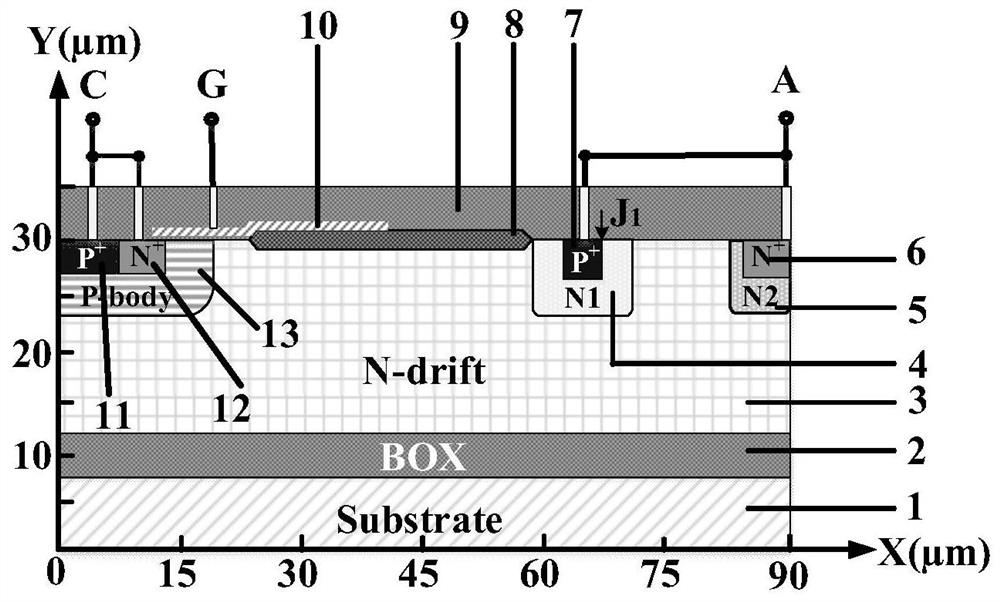
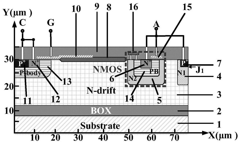
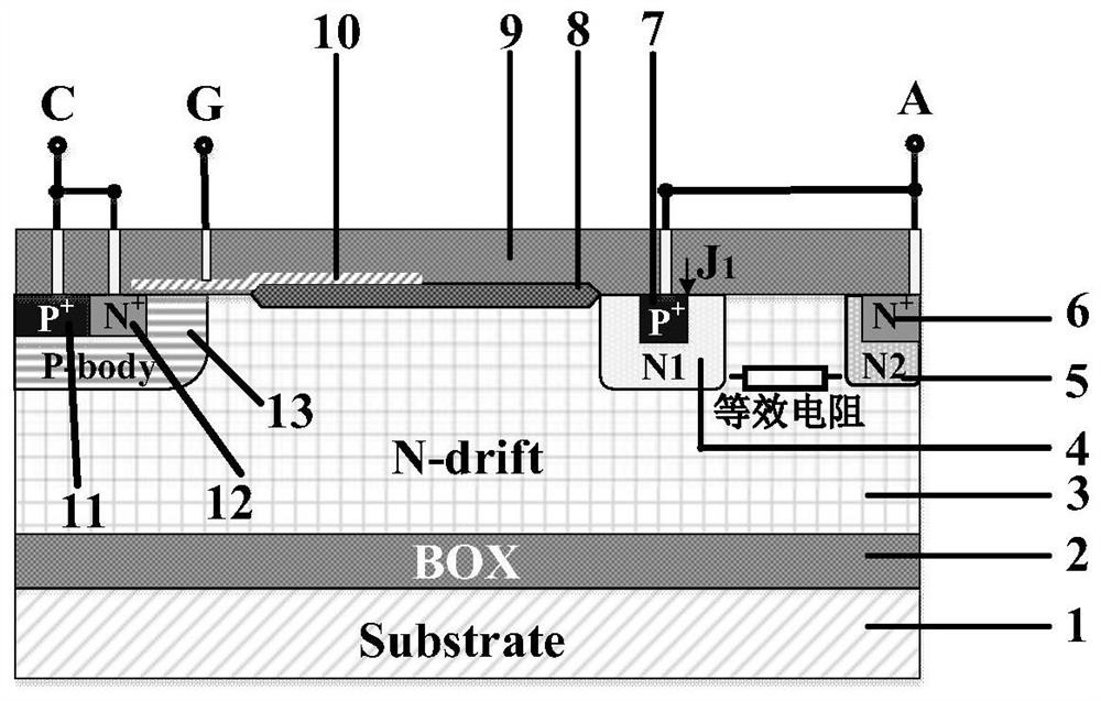
[0023] An anode short-term laterally insulated gate bipolar transistor that eliminates the negative resistance effect, including the p-type substrate 1, provided with an oxidation layer 2 on the P-shaped substrate 1, and N is provided on the oxide laid 2 The type drift zone 3 is characterized in that the silica oxide layer 9 is provided on the surface of the n-type drift region 3, and a lateral insulated gate bipolar transistor and an N metal oxide semiconductor field are provided in the n-type drift region 3. Effect transistor, the lateral insulated gate bipolar transistor includes a first n-type heavy doped region 4 provided in the n-type drift region 3 and the first n-type heavy doped region 4 is located on the surface of the n-type drift region 3, A P-type retracting anode region 7 is provided in the first N-type heavy doping region 4, and the n-type metal oxide semico...


PUM


Abstract

An anode short-circuit lateral insulated gate bipolar transistor for eliminating the negative resistance effect, comprising a P-type substrate, an oxide buried layer is arranged on the P-type substrate, and an N-type drift region is arranged on the oxide buried layer, It is characterized in that a silicon dioxide oxide layer is provided on the surface of the N-type drift region, LIGBT and NMOS are arranged in the N-type drift region, the LIGBT includes a first N-type heavily doped region, and the first N-type heavily doped A P-type heavily doped anode region is provided in the doped region, and the NMOS includes a second N-type heavily doped region, a P-type well region is arranged in the second N-type heavily doped region, and a P-type well region is arranged in the P-type well region. Surrounded by an N-type heavily doped anode region, the second N-type heavily doped region is electrically connected to the P-type well region, and a polysilicon gate is provided in the silicon dioxide oxide layer, and the polysilicon gate is heavily doped from N-type The upper region of the anode region crosses the P-type well region and enters the upper region of the second N-type heavily doped region, and the polysilicon gate is also connected with the N-type heavily doped anode region and the P-type heavily doped anode region.

Description

Technical field [0001] The present invention mainly relates to the field of power semiconductor device, and is an anode short-path lateral insulated gate bipolar transistor that eliminates the negative resistance effect. Background technique [0002] The lateral insulated gate bipolar transistor (LIGBT) is a composite power device that evolved in the MOS gate device structure and the bipolar transistor structure, which has a MOS field effect transistor and a bipolar transistor. Features, it is easy to integrate, high withstand voltage, strong driving current capability, and wide application in power integrated circuits. In bridge circuit applications, LIGBT is often used as a switch tube, but the traditional LIGBT has a severe tail current phenomenon, so that it is slower, and the turn-off loss is too high, which seriously limits its in high frequency field. The application, at the same time, the bridge circuit is used in the process of changing, and the fast recovery diode needs...

Claims


Application Information

Patent Timeline
Patent Type & Authority Patents(China)
IPC IPC(8): H01L29/06H01L29/40H01L29/423H01L29/739
CPCH01L29/7394H01L29/0684H01L29/40H01L29/423
Inventor 祝靖邹艳勤李少红孙伟锋陆生礼时龙兴
Owner SOUTHEAST UNIV
Features
  • R&D
  • Intellectual Property
  • Life Sciences
  • Materials
  • Tech Scout
  • Unparalleled Data Quality
  • Higher Quality Content
  • 60% Fewer Hallucinations
Learn More