Transverse insulated gate bipolar transistor with low turn-on overshoot current

A bipolar transistor, overshoot current technology, applied in the direction of thyristor, circuit, electrical components, etc., can solve the problems of slowing down the switching speed of the device, increasing the gate area, and high current peak value, achieving easy process, low production cost, The structure makes simple effects

Active Publication Date: 2019-08-30
SOUTHEAST UNIV
View PDF4 Cites 3 Cited by
  • Summary
  • Abstract
  • Description
  • Claims
  • Application Information

AI Technical Summary

Problems solved by technology

However, the U-shaped channel inevitably increases the area of ​​the gate, resulting in an increase in gate capacitance
In the double-pulse test, the SOI-LIGBT device with U-shaped channel has obvious gate voltage overshoot, causing the current peak value flowing through the device to be too high when the second pulse is ...

Method used


Image

  • Transverse insulated gate bipolar transistor with low turn-on overshoot current
  • Transverse insulated gate bipolar transistor with low turn-on overshoot current
  • Transverse insulated gate bipolar transistor with low turn-on overshoot current

Examples


Embodiment Construction

[0029] Combine below Figure 4 , Figure 5 , Figure 6 , Figure 7 , the present invention is described in detail:

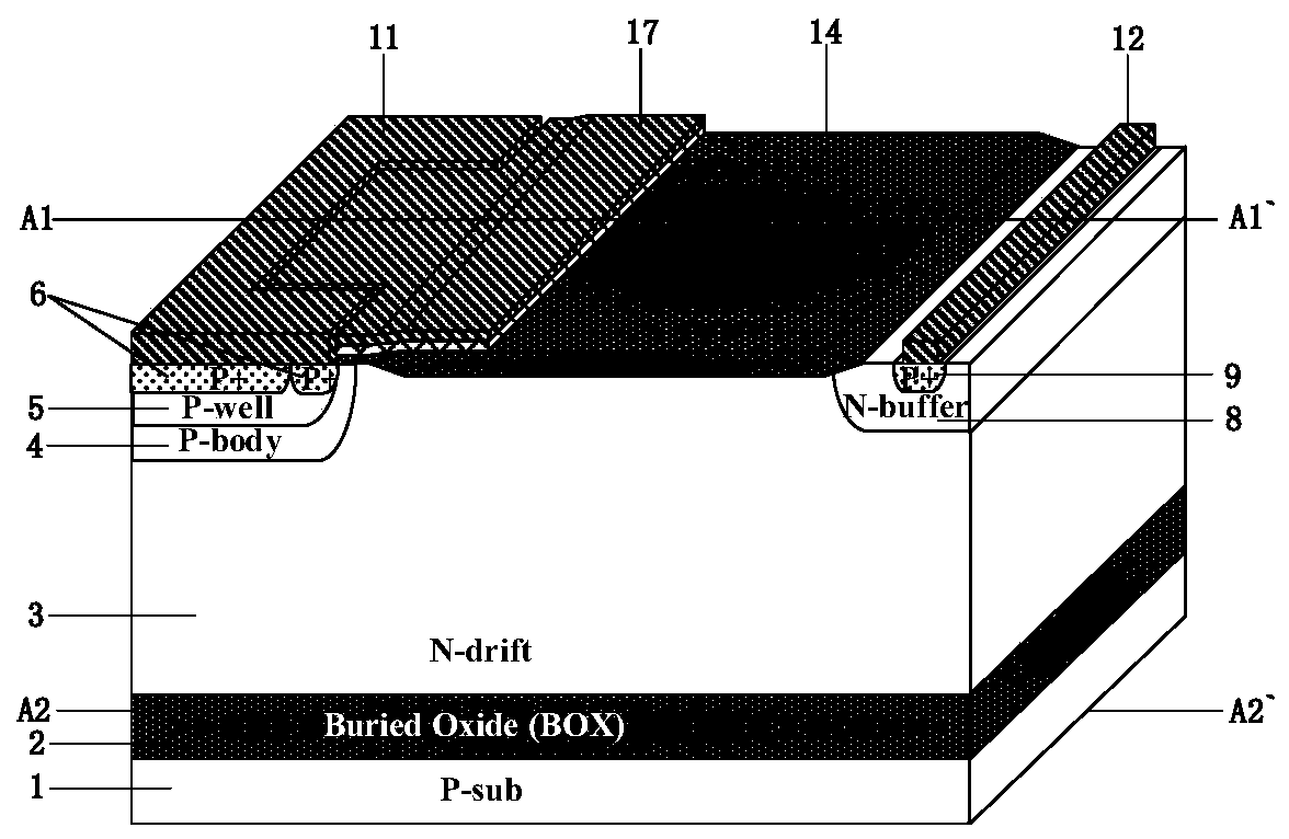
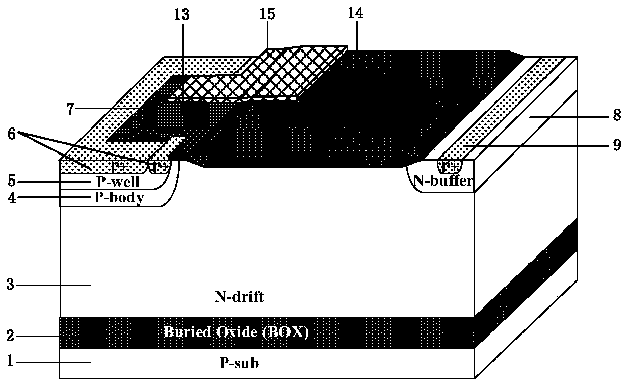
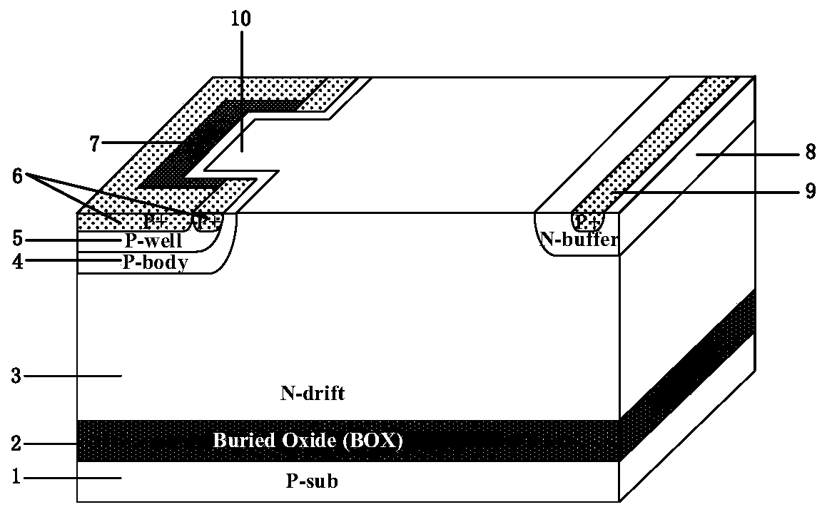
[0030]A lateral insulated gate bipolar transistor with low turn-on overshoot current, comprising: a P-type substrate 1, a buried oxide layer 2 is arranged on the P-type substrate 1, and an N-type drift is arranged on the buried oxide layer 2 Zone 3, a P-type body zone 4 and an N-type buffer zone 8 are respectively provided on both sides of the N-type drift zone 3, a field oxide layer 14 is provided above the N-type drift zone 3, and a field oxide layer 14 is provided in the N-type buffer zone 8. There is a heavily doped P-type collector region 9, and a collector metal 12 is connected to the heavily doped P-type collector region 9, and the collector metal 12 is connected to the first peripheral terminal 19a, and in the P-type body region 4 There is a P-type well region 5 inside, and a heavily doped P-type emitter region 6 and a heavily doped N-type emitter re...


PUM

PropertyMeasurementUnit
Widthaaaaaaaaaa
Resistanceaaaaaaaaaa

Abstract

The invention relates to a transverse insulated gate bipolar transistor with low turn-on overshoot current, which reduces the peak current flowing through the device when the second gate pulse is turned on under the premise of maintaining the current capacity and voltage withstanding capacity. According to the semiconductor, a buried oxide is arranged on a P-type substrate, an N-type drift regionis arranged on the buried oxide, a P-type body region and an N-type buffer region are arranged on the N-type drift region, the N-type buffer region is internally provided with a P-type collector region, a field oxide layer is arranged on the N-type drift region, the P-type body region is internally provided with a P-type well region, the P-type well region is internally provided with a P-type emitter region and an emitter region, and the inner side boundaries of the above four regions are synchronously recessed inwardly to form a pinch-off region. The surface of the P-type body region is provided with a gate oxide layer, a polycrystalline silicon gate electrode is arranged on the gate oxide layer, the polycrystalline silicon gate electrode is composed of a first gate electrode located on the surface of the P-type body region and a second gate electrode located on the pinch-off region and the N-type drift region, the first gate electrode is connected with a first gate resistor, and thesecond gate electrode is connected with a second gate resistor.

Description

technical field [0001] The invention mainly relates to the technical field of power semiconductor devices, is a lateral insulated gate bipolar transistor with low turn-on overshoot current, and is especially suitable for single-chip integrated intelligent power chips. Background technique [0002] Silicon-on-Insulator Lateral Insulated Gate Bipolar Transistor (Silicon-on-Insulator Lateral Insulated Gate Bipolar Transistor, referred to as SOI-LIGBT), has the advantages of easy integration, high withstand voltage, and fast switching speed, and is widely used in monolithic integrated smart power chips middle. The current capability of SOI-LIGBT devices is a key factor affecting the power consumption and area of ​​monolithic integrated smart power chips. In order to improve the current capability of the device, a U-shaped channel can be used to increase the effective channel width, thereby improving the current capability of the device. However, the U-shaped channel inevitably...

Claims


Application Information

Patent Timeline
IPC IPC(8): H01L29/739H01L29/423
CPCH01L29/7394H01L29/423H01L29/0696H01L29/1095H01L29/402H01L29/083
Inventor 张龙李安康祝靖孙伟锋陆生礼时龙兴
Owner SOUTHEAST UNIV
Why Eureka
Try Eureka