
Full-color emitting LED epitaxial structure based on GaN hexagonal prism array and preparation method of epitaxial structure

A technology of epitaxial structure and hexagonal truss, which is applied in the field of epitaxial structure and preparation of full-color emission LED, can solve the problem that the in-situ deposition mask of phosphor powder conversion efficiency is difficult to accurately control the size and distribution of GaN micro/nano arrays, and achieve improvement The effect of internal quantum efficiency, avoiding sudden drop in efficiency, and reducing threading dislocation density

Inactive Publication Date: 2019-09-06
TAIYUAN UNIV OF TECH
View PDF4 Cites 3 Cited by
  • Summary
  • Abstract
  • Description
  • Claims
  • Application Information

AI Technical Summary

Problems solved by technology

[0003] The present invention aims at the problems of phosphor powder conversion efficiency and in-situ deposition mask that are difficult to accurately control the size and distribution of GaN micro / nano arrays in the prior art, and provides a full-color emitting LED epitaxial structure and preparation method based on GaN hexagonal frustum arrays

Method used


Image

  • Full-color emitting LED epitaxial structure based on GaN hexagonal prism array and preparation method of epitaxial structure
  • Full-color emitting LED epitaxial structure based on GaN hexagonal prism array and preparation method of epitaxial structure
  • Full-color emitting LED epitaxial structure based on GaN hexagonal prism array and preparation method of epitaxial structure

Examples


Embodiment Construction

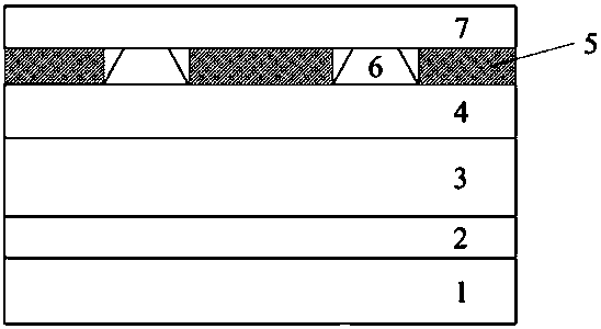
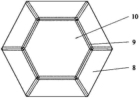
[0035] This embodiment provides a full-color emission LED epitaxial structure based on a GaN hexagonal truss array, such as figure 1 As shown, from bottom to top, it includes sapphire substrate 1, nucleation layer 2, undoped GaN layer 3, n-type GaN layer 4, patterned SiO 2Mask layer 5; n-type GaN hexagonal truss array 6 in the gap of the patterned mask layer, and multi-quantum on six semipolar (10-11) crystal planes located on the top surface of the hexagonal truss (0001) The well layer 8, the quantum wire 9 on the edge, the quantum dot 10 on the top surface, and finally the p-type GaN layer 7.

[0036] The three-dimensional structure composed of GaN hexagonal platform array and multi-quantum well layer 8, quantum wire 9 and quantum dot 10 on each outer surface has a large light-emitting area. Compared with thin-film materials, it can generate more light at the same current density. The number of photons increases the internal quantum efficiency of the LED epitaxial structure...


PUM

PropertyMeasurementUnit
Thicknessaaaaaaaaaa
Thicknessaaaaaaaaaa
Thicknessaaaaaaaaaa

Abstract

The invention relates to a full-color emitting LED epitaxial structure based on a GaN hexagonal prism array and a preparation method of the epitaxial structure, belongs to the technical field of semiconductors, and can solve the problem that in the prior art, the fluorescent powder conversion efficiency is low, and it is difficult to accurately control an in-situ deposition mask and the GaN micron / nano array dimension and distribution; the epitaxial structure comprises a sapphire substrate, a nucleation layer, a non-doped GaN layer, an n-type GaN layer, a patterned SiO2 mask layer, an n-type GaN hexagonal prism array at the gap of the patterned SiO2 mask layer, quantum dots located at the top surface of the hexagonal prism, quantum wires on the edges, and a multi-quantum-well layer on a top surface (0001) crystal surface and six half-polarity (10-11) crystal surfaces, and a final p type GaN layer. By virtue of the structure, the GaN micron / nano array dimension and distribution can be accurately controlled, the problems that a stark effect is limited by the quantum well, the efficiency is lowered suddenly, the light-emitting wavelength is single and the like in the two-dimensional GaN-based thin film LED can be solved, and full-color emission is realized.

Description

technical field [0001] The invention belongs to the technical field of semiconductors, and in particular relates to a full-color emitting LED epitaxial structure and a preparation method based on a GaN hexagonal truss array. Background technique [0002] As a new generation of lighting equipment, LED has many advantages such as high brightness, low cost, long life, small size, energy saving and environmental protection. At present, white light LEDs are mainly realized in the following three ways: the first is to obtain white light by exciting phosphors with ultraviolet LEDs. This method is similar to the principle of fluorescent lamps. Ultraviolet LEDs can generate longer wavelengths through organic or inorganic phosphors. Visible light ranging from blue to red light can be obtained, thus enabling white light emission. The second is achieved by exciting phosphors with blue light. Part of the blue light is transmitted through the phosphor, and the other part is absorbed by ...

Claims


Application Information

Patent Timeline
IPC IPC(8): H01L33/20H01L33/24H01L33/02H01L33/06H01L33/16H01L33/32H01L33/00B82Y40/00
CPCB82Y40/00H01L33/007H01L33/025H01L33/06H01L33/16H01L33/20H01L33/24H01L33/325
Inventor 贾伟张利繁党随虎李天保董海亮许并社
Owner TAIYUAN UNIV OF TECH
Learn More