

Method of producing semiconductor epitaxial wafer
- Summary
- Abstract
- Description
- Claims
- Application Information
AI Technical Summary
Problems solved by technology
Method used
Image

Examples
Embodiment
[0085] (trial example 1)
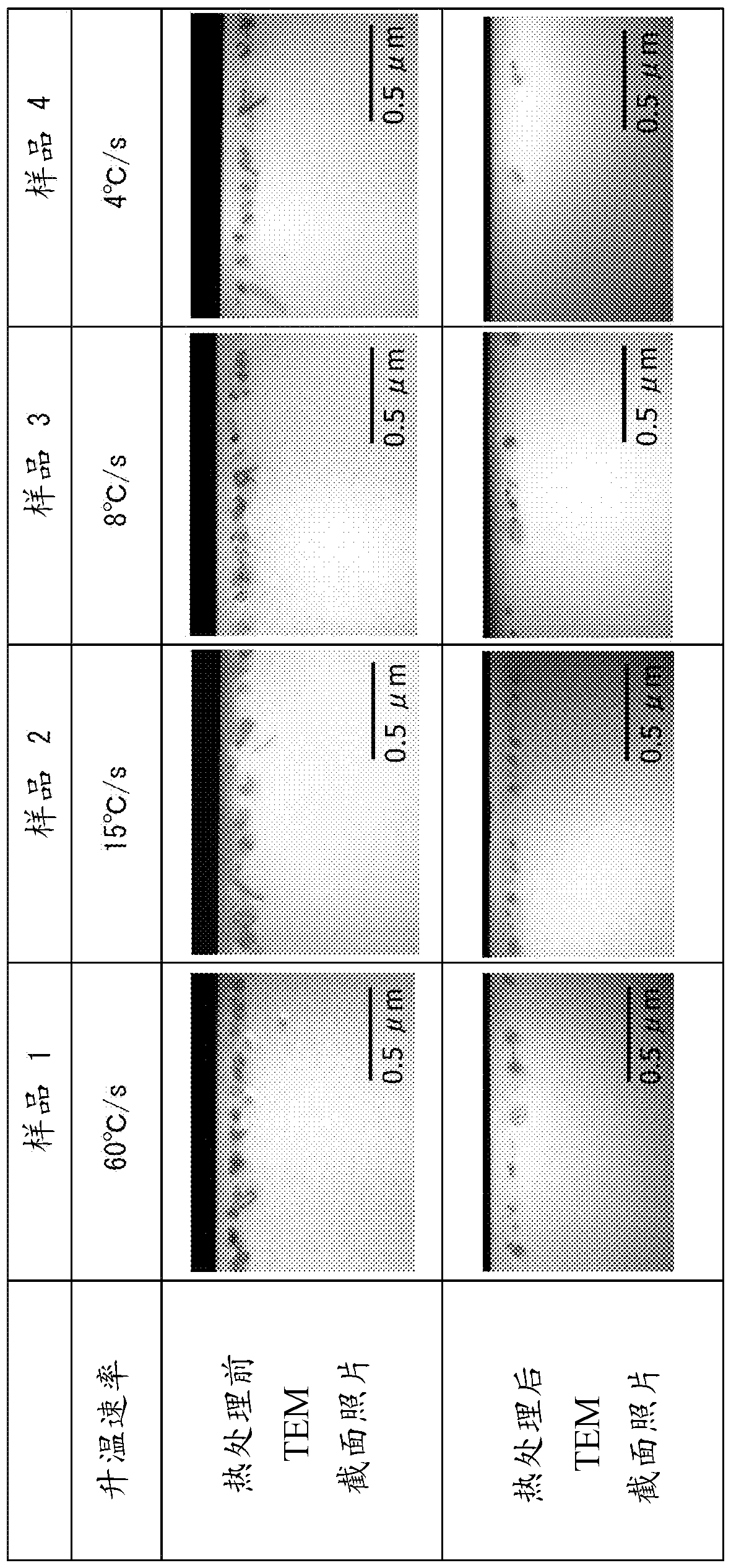
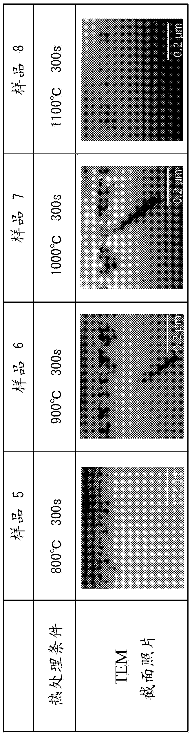
[0086] A silicon wafer (diameter: 300 mm, thickness: 725 μm, dopant type: phosphorus, resistivity: 10 Ω·cm) obtained from a CZ single crystal silicon ingot was prepared. Next, using a cluster ion generator (manufactured by NISSIN ION EQUIPMENT CO., LTD., model: CLARIS (registered trademark)), the surface of the silicon wafer was irradiated with diethyl ether (C 4 h 10 O) cluster ionized by CH 3 Multi-element cluster ions composed of O. In addition, the dose of the cluster ion was set to 1.0×10 15 Cluster / cm 2 (The carbon dose is also 1.0×10 15 atoms / cm 2 ).
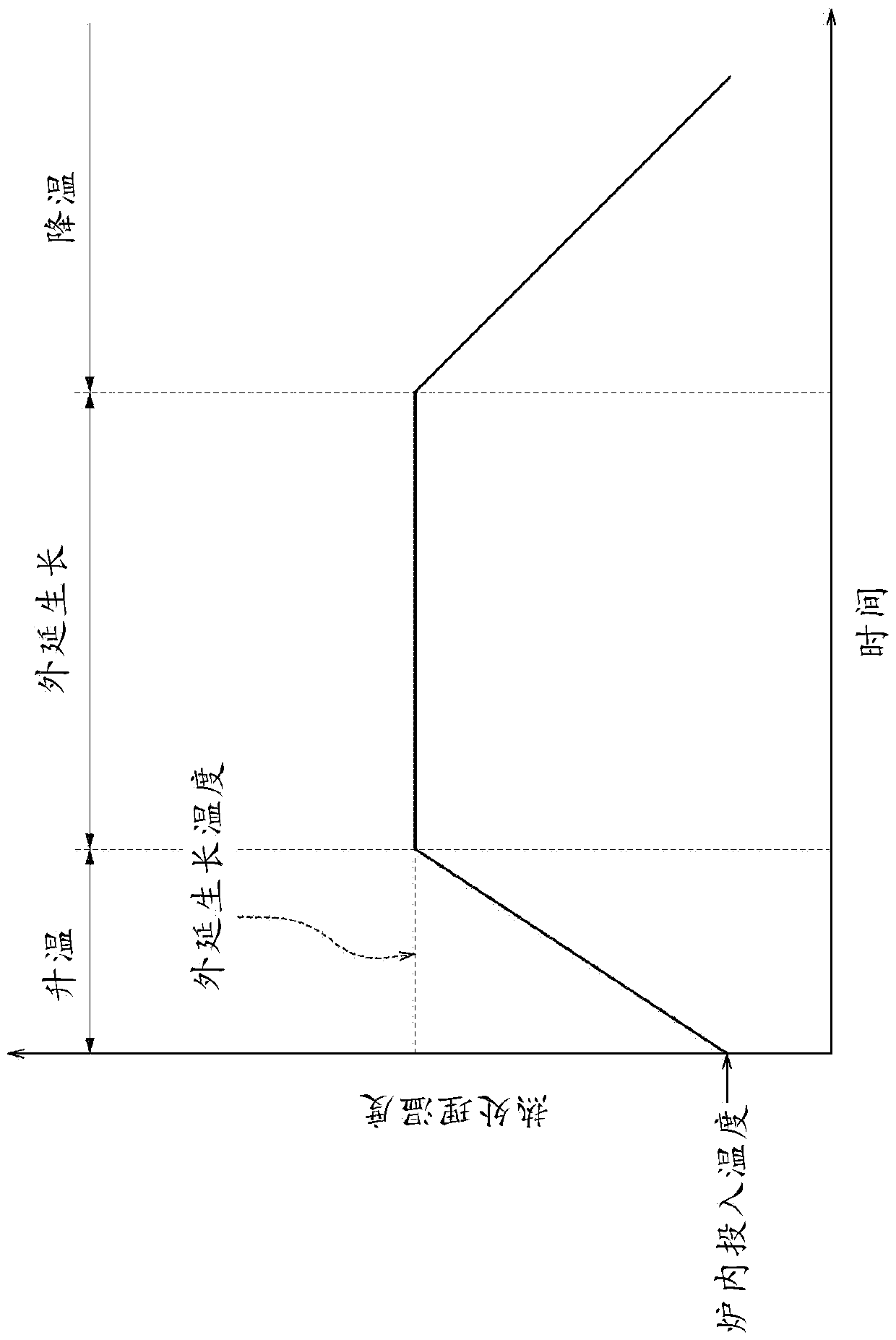
[0087] Next, the above-mentioned silicon wafer was transferred to a monolithic epitaxial growth apparatus (manufactured by APPLIED MATERIALS, INC.) at a furnace temperature of 600°C. Next, the heating time up to 800° C. is set to 5 seconds (the heating rate is 40° C. / s), and the heating time from 800° C. to 1000° C. is set to 5 seconds (the heating rate is 40° C. / s). Raise the temperat...
PUM
| Property | Measurement | Unit |
|---|---|---|
| diameter | aaaaa | aaaaa |
| thickness | aaaaa | aaaaa |
| electrical resistivity | aaaaa | aaaaa |
Abstract
Description
Claims
Application Information