Deep ultraviolet LED chip and preparation method thereof

An LED chip, deep ultraviolet technology, applied in semiconductor devices, electrical components, circuits, etc., can solve the problems affecting the contact performance of N-type ohmic contact electrodes, chip current accumulation, damage to ohmic contacts, etc., to improve light extraction efficiency, avoid Influence each other and reduce the effect of absorption

Active Publication Date: 2019-09-20
JIANGXI ZHAO CHI SEMICON CO LTD
View PDF5 Cites 7 Cited by
  • Summary
  • Abstract
  • Description
  • Claims
  • Application Information

AI Technical Summary

Problems solved by technology

However, P-type GaN has a strong absorption effect on deep ultraviolet light, which reduces the light extraction efficiency of deep ultraviolet LED chips.
[0004] (2) In addition, the ohmic contact between N-type AlGaN and N electrode metal needs to be formed at a higher temperature, and high temperature annealing will destroy the ohmic contact formed between P-type AlGaN and P electrode metal
In order to avoid this effect, the N-type ohmic contact electrode can be prepared first, and then the P-type ohmic contact electrode is prepared, but at this time, the annealing process of the P-type ohmic contact electrode will also affect the contact performance of the N-type ohmic contact electrode.
[0005] (3) The resistivity of AlGaN material with high Al composition is high. When the injection current of deep ultraviolet LED chip is large, the chip current accumulation phenomenon will be more serious.
[0006] In the prior art, the P electrode and the N electrode of the LED chip are often prepared on a conductive substrate at the same time, so that the two electrodes will affect each other during the annealing process, and it is difficult to achieve a balance. Therefore, there is an urgent need for a technology that can combine the P electrode and the N electrode. The electrodes are prepared separately to reduce the mutual influence of annealing and reduce the chip current aggregation phenomenon

Method used


Image

  • Deep ultraviolet LED chip and preparation method thereof
  • Deep ultraviolet LED chip and preparation method thereof
  • Deep ultraviolet LED chip and preparation method thereof

Examples


Embodiment 1

[0073] The structure and specific implementation steps of the deep ultraviolet LED chip provided by Embodiment 1 of the present invention are as follows:

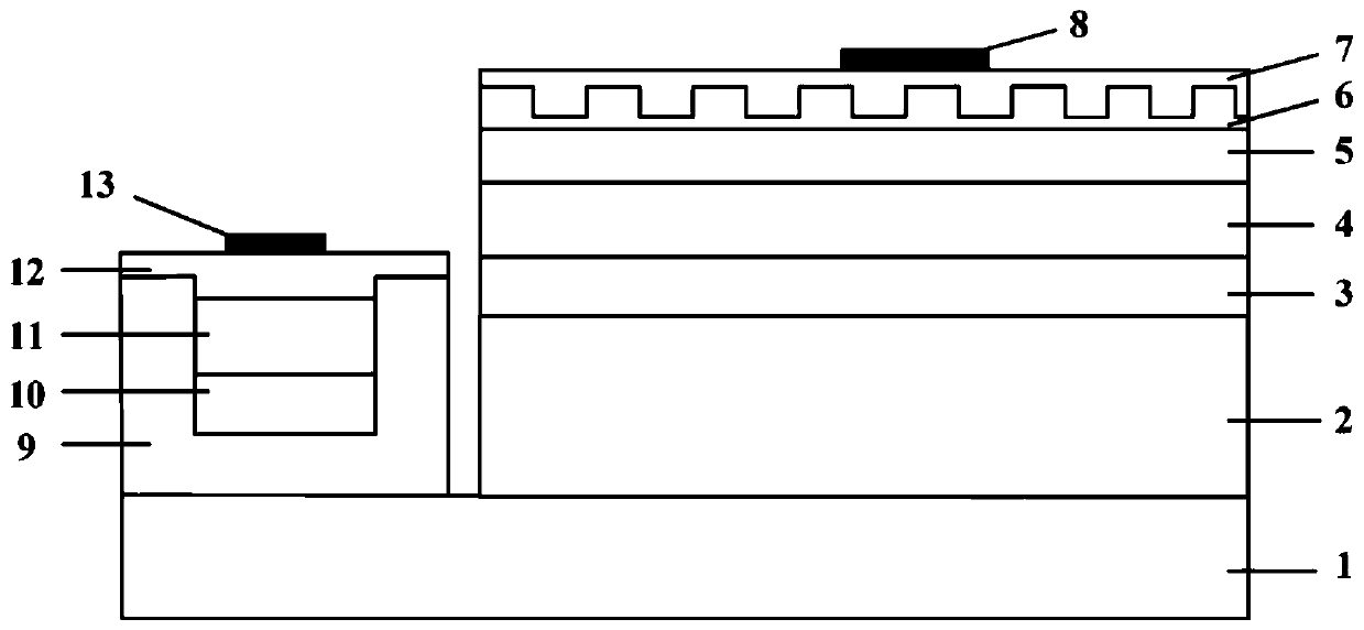
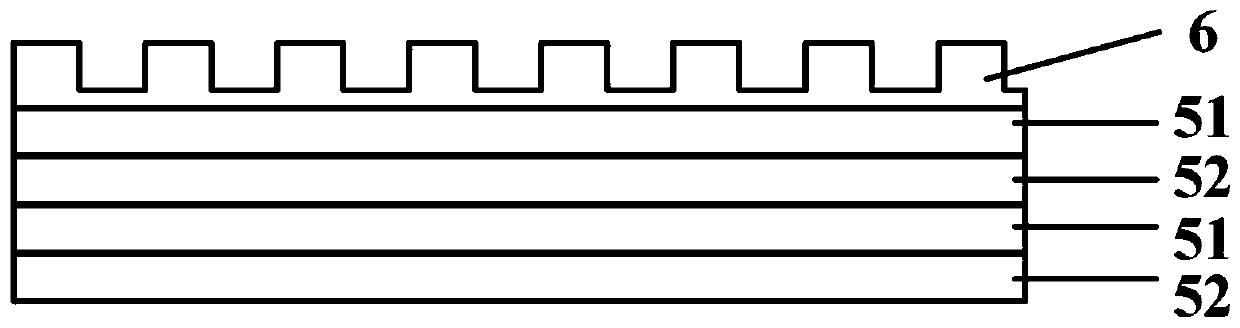
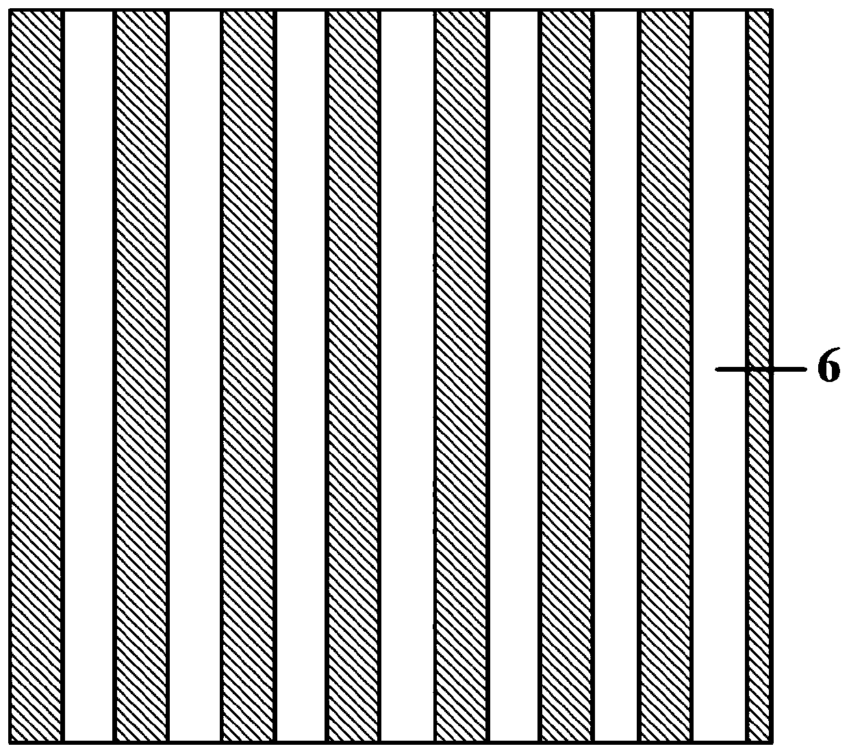
[0074] (1) Prepare conductive substrate 1, and divide P electrode area and N electrode area on conductive substrate 1; On the P electrode area of ​​conductive substrate 1, grow the epitaxial structure of deep ultraviolet LED chip, prepare P electrode, conductive lining Bottom 1 can be made of SiC, P-type doped Si and other materials, refer to figure 1 , the epitaxial structure includes: N-type AlGaN layer 2 , multiple quantum well layer 3 , P-type AlGaN layer 4 , AlN / GaN superlattice ohmic contact layer 5 , and P-type GaN layer 6 . refer to figure 2 , wherein the AlN / GaN superlattice ohmic contact layer 5 is composed of atomically thick AlN layers 51 and GaN layers 52 arranged alternately, and the AlN layer 51 and GaN layer 52 can be doped with Mg to improve the ohmic contact performance, and the P-type GaN The thickness...

Embodiment 2

[0086] The structure and specific implementation steps of the deep ultraviolet LED chip provided by Embodiment 2 of the present invention are as follows:

[0087] (1) Prepare the conductive substrate 14, and divide the P electrode region and the N electrode region on the conductive substrate 1; grow the epitaxial structure of the deep ultraviolet LED chip on the insulating substrate 31, prepare the P electrode, and the insulating substrate 31 can adopt Sapphire, SiO 2 material, see Figure 5 , and its structure includes: N-type AlGaN layer 2, multiple quantum well layer 3, P-type AlGaN layer 4, AlN / GaN superlattice ohmic contact layer 5, and P-type GaN layer 6. refer to figure 2 , wherein the AlN / GaN superlattice ohmic contact layer 5 is composed of atomically thick AlN layers 51 and GaN layers 52 alternately arranged, and the AlN layer 51 and GaN layer 52 can be doped with Mg to improve the ohmic contact performance. The thickness of the p-type GaN layer 6 is 10-15 nm.

...


PUM


Abstract

The present invention discloses a deep ultraviolet LED chip and a preparation method thereof. An N electrode of the deep ultraviolet LED chip comprises an N-type AlGaN layer, a multiple quantum well layer, a P-type AlGaN layer, an AlN / GaN superlattice ohmic contact layer and a P-type GaN layer. The AlN / GaN superlattice is composed of a doped or undoped AlN layer and GaN layer with a thickness of an atomic layer level; the P-type GaN layer is etched by the photolithography methods such as laser direct writing to form a nano-scale periodic pattern; and an evaporated transparent conductive layer and a P electrode pad composed of multiple layers of metal are prepared on the P-type GaN layer. The N electrode is a tunnel junction composed of a lightly doped P<->-type AlGaN layer, a heavily doped P<++>-type AlGaN layer, a heavily doped N<++>-type AlGaN layer and a lightly doped N<->-type AlGaN layer; and an N-electrode pad, an N electrode and a P electrode are separately prepared on the tunnel junction and then bonded to a conductive substrate. The invention improves the light extraction efficiency of the deep ultraviolet LED chip and enhances the current expansion performance and thermal diffusion performance of the deep ultraviolet LED chip.

Description

technical field [0001] The invention belongs to the field of semiconductor luminescence, and relates to an LED chip, in particular to a deep ultraviolet LED chip and a preparation method thereof. Background technique [0002] Deep ultraviolet LED chips have great application value and prospects in water and air purification, biomedicine, optical communication, and high-density storage. [0003] (1) Due to the large forbidden band width of the P-type AlGaN material, the contact barrier formed with the metal is relatively high. Not only that, as the molar composition of Al atoms increases, the height of the contact barrier will also increase, making it difficult to form a low-resistance ohmic contact between the metal and the high Al composition P-type AlGaN, thus affecting the photoelectric performance of the UV LED chip. . Therefore, a P-type GaN layer is usually prepared on the P-type AlGaN to improve the ohmic contact performance between the metal and the P-type GaN. Ho...

Claims


Application Information

Patent Timeline
Patent Type & Authority Applications(China)
IPC IPC(8): H01L33/06H01L33/24H01L33/32H01L33/38H01L33/00
CPCH01L33/0075H01L33/0093H01L33/06H01L33/24H01L33/325H01L33/38
Inventor 周圣军刘梦玲徐浩浩
Owner JIANGXI ZHAO CHI SEMICON CO LTD
Why Eureka
Try Eureka